
A precision temperature sensor looks stable on the bench, then begins to wander when a nearby motor starts. An audio preamplifier produces a faint buzz only after it is installed in a metal enclosure. A microcontroller resets at random, even though its supply voltage appears correct on a handheld meter.
These are familiar failures because electrical noise is rarely a single, obvious defect. It is usually an unwanted signal finding a path through power wiring, a ground connection, a cable, the air, or even the circuit board itself.
For sensitive electronic circuits, noise can hide small signals, corrupt data, reduce measurement accuracy, and create intermittent faults that are expensive to diagnose. The challenge is not simply to add a capacitor or shield everything; it is to understand the source, the coupling path, and the circuit’s susceptibility.
Once those three pieces are separated, noise control becomes a practical engineering process rather than trial and error.
⚡ What Electrical Noise Really Means
Electrical noise is any unwanted voltage or current that interferes with the signal or power a circuit is meant to use. It may be periodic, such as 50 Hz or 60 Hz mains hum, or irregular, such as broadband switching noise from a converter.
Noise is not necessarily random. A clock edge, relay contact, PWM motor drive, or radio transmitter can create a repeatable disturbance. It becomes “noise” when it appears in the wrong place and prevents useful operation.
🎯 Why Sensitive Circuits Are Vulnerable
A circuit is sensitive when its wanted signal is small, its timing margin is narrow, or its decision threshold is easily crossed. A microphone preamplifier may work with microvolt-level inputs, while a high-speed digital receiver may care about nanoseconds of timing error.
The same interference that has no visible effect on an LED driver can overwhelm a strain-gauge amplifier. Noise performance must therefore be judged against the circuit’s signal amplitude, bandwidth, impedance, and required accuracy.
🧭 The Source-Path-Victim Model
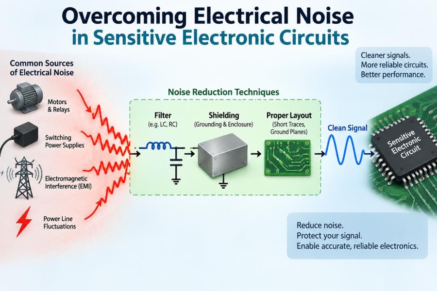
A useful troubleshooting model has three parts: a source generates interference, a coupling path carries it, and a victim responds to it. Breaking any one of these parts can solve the problem.
For example, a switching regulator may be the source, a shared ground impedance may be the path, and an analog-to-digital converter reference may be the victim. Replacing the converter may not help; rerouting its return current often does.
🌊 Common Forms of Circuit Noise
Noise is easier to manage when its character is identified. A low-frequency sine-like ripple calls for a different investigation from narrow spikes that occur at every switching transition.
- Thermal noise: unavoidable random motion of charge carriers in resistors and other conductive materials.
- Shot noise: current fluctuation associated with discrete charge flow, especially in semiconductor junctions.
- Flicker noise: low-frequency “1/f” noise that matters in precision amplifiers and sensors.
- Conducted noise: disturbance traveling through wires, traces, power rails, or grounds.
- Radiated noise: energy coupled through electric or magnetic fields.
🔥 Thermal Noise Sets a Physical Floor
Every resistor produces thermal noise, even with an ideal power supply and perfect layout. The amount rises with resistance, temperature, and measurement bandwidth.
This does not mean low resistance is always best. Lower resistance increases current consumption and may load a sensor or source. The practical goal is to choose impedances that meet power and signal requirements without needlessly raising the noise floor.
📉 Bandwidth Determines How Much Noise Arrives
Many noise sources spread energy across a wide range of frequencies. A circuit that listens over a wide bandwidth collects more of that energy than one that passes only the frequencies it needs.
A slow-moving temperature measurement does not need a wideband amplifier path. Limiting bandwidth with an analog low-pass filter, followed by sensible digital averaging, can greatly improve stability without losing useful information.
🔄 Switching Regulators and Fast Edges
Switch-mode power supplies are efficient, but their rapidly changing currents and voltages create harmonics well beyond the nominal switching frequency. The troublesome energy often comes from short transition edges, ringing, and current loops rather than the fundamental frequency alone.
Good converter layout keeps the high-current switching loop physically small. Input capacitors must sit close to the switching device, and the noisy switch node should be kept away from sensitive traces, connectors, and analog circuitry.
⚙️ Digital Logic Is a Noise Source Too
Digital signals are often described as clean zeros and ones, but every transition draws transient current. A fast output edge can inject noise into the supply, create ground bounce, and capacitively couple into adjacent traces.
Clock frequency is not the whole story. A modest-frequency signal with very fast rise time can radiate and couple more strongly than expected. Where timing permits, slowing edges with a small series resistor can reduce ringing and emissions.
🏭 Motors, Relays, and Inductive Loads
Motors, solenoids, relays, and long cable loads store energy in magnetic fields. When current is interrupted, that energy produces a voltage transient that may be far larger than the normal supply voltage.
Use an appropriate suppression method at the load: a flyback diode for many DC coils, or a suitably designed snubber, transient suppressor, or other network when release time or AC operation makes a simple diode unsuitable. Selection depends on the load and switching requirements.
🔌 Conducted Noise on Power Rails
Power wires have resistance and inductance. When a load current changes, the voltage at another circuit can shift because both circuits share part of the same supply path.
This is why a sensor may become noisy when a display backlight turns on. Separate branch routing, local energy storage, and filtering can keep pulsed load current from modulating the rail seen by sensitive electronics.
🪨 Ground Is Not an Ideal Zero-Volt Node
On a schematic, every ground symbol may look identical. On a real board, copper has impedance, especially at high frequency. Current flowing through a shared return segment creates a voltage drop, and another circuit may interpret that drop as part of its signal.
This mechanism is often called common-impedance coupling. It explains many failures blamed vaguely on “bad grounding.” The meaningful question is: which current shares which return path?
🧩 Return Paths Follow Signal Paths
A signal current always needs a return path. At low frequency, it may spread through available ground conductors. At high frequency, it tends to return close to the outgoing path because that minimizes loop inductance.
A continuous ground plane underneath a fast trace provides a short, predictable return path. Splitting that plane beneath the trace can force return current around the gap, increasing loop area, radiation, and susceptibility.
🧱 Ground Planes and Partitioning
A solid ground plane is usually more useful than dividing a board into many isolated ground islands. Splits are sometimes justified by safety, high-voltage isolation, or carefully controlled system architecture, but they can easily create return-path problems.
Partition components by function instead: keep switching power components together, keep low-level analog inputs away from them, and control where noisy and quiet currents meet. The objective is current containment, not decorative separation.
🪢 Ground Loops in Connected Systems
A ground loop occurs when two grounded pieces of equipment have more than one conductive return path. Small voltage differences between those paths can drive unwanted current through a cable shield or signal return.
Audio hum is a classic example, but industrial sensors can suffer similarly. Differential signaling, galvanic isolation, carefully chosen shield termination, and a deliberate grounding scheme can reduce the problem. The best choice depends on frequency, safety requirements, and installation conditions.
🧲 Magnetic Coupling and Loop Area
A changing magnetic field can induce voltage in a loop of wire or copper. Large loops are more exposed, which is why a sensor pair routed apart can pick up interference from a transformer or motor cable.
Twisting the two conductors reduces the loop area and makes induced interference more nearly equal in both wires. A differential receiver can then reject much of the shared disturbance.
☁️ Capacitive Coupling Between Conductors
Conductors separated by insulation form a small capacitor. A fast-changing voltage on one conductor can push current through that capacitance into a nearby high-impedance node.
This is common when a high-voltage switching node runs beside a sensitive analog trace. Increasing separation, adding a grounded guard or plane, reducing source edge speed, and lowering victim impedance where practical all reduce the effect.
📡 Radiated Interference and Antenna Behavior
Any wire, cable, or trace can behave partly like an antenna at some frequencies. Long external cables are especially effective at collecting interference and carrying it into equipment.
At board level, fast current loops and poorly terminated cable shields can also radiate. A metal enclosure may help, but it works best when cable entry, seams, bonding, and internal return paths are treated as part of the same electromagnetic design.
🛡️ Shielding Has Limits
A conductive shield is most effective against electric-field coupling when it is properly bonded. Magnetic fields at low frequency can be harder to block, particularly strong fields from transformers or high-current conductors.
A shield is not a substitute for good routing. If noise is already conducted onto a reference or power rail inside the enclosure, adding a metal box around the assembly may make little difference.
📏 Differential Signaling and Common-Mode Rejection
A differential input measures the voltage difference between two conductors rather than one conductor relative to ground. Noise coupled equally onto both lines is called common-mode noise and can be rejected within the input’s specified operating range.
Rejection is not unlimited. Impedance mismatch, unequal cable coupling, excessive common-mode voltage, and poor PCB routing convert common-mode interference into differential error. Matched trace routing and balanced source impedances preserve the benefit.
🎛️ Choosing the Right Filter
Filters should be designed around the wanted signal and the actual interference spectrum. A low-pass filter suits a slow sensor; a notch filter may address a known narrow-frequency tone; a common-mode choke can attenuate interference on paired cable conductors.
| Noise situation | Typical useful approach | Key caution |
|---|---|---|
| Slow sensor with high-frequency ripple | Low-pass filtering near the input | Do not make response slower than the application permits |
| Switching noise on a supply rail | Local decoupling plus layout improvement | A capacitor cannot compensate for a large current loop |
| Interference on a long cable | Twisted pair, shielding, common-mode filtering | Shield termination must match the frequency and system grounding |
| Digital trace ringing | Series termination or controlled impedance routing | Verify timing after changing edge rate |
🧪 Decoupling Capacitors Need Placement
A decoupling capacitor supplies brief current locally when an IC changes state. Its usefulness depends on low impedance over the needed frequency range and, critically, a short connection to the IC power and ground pins.
A capacitor placed far away can be separated by trace inductance, making it ineffective during fast transients. Use local ceramic capacitors as recommended for the device, then add bulk capacitance where slower load changes require stored energy.
🧰 Ferrite Beads, Chokes, and Their Trade-Offs
Ferrite beads can present high impedance to high-frequency noise while passing DC. They are useful for isolating a local analog supply or reducing cable-borne interference, but they are not universal fixes.
With capacitors, a bead can create resonances or reduce regulator stability if used without checking the power network. Review impedance-versus-frequency data, DC bias behavior, and the regulator’s output-capacitor requirements rather than selecting by package size alone.
🧮 ADC References and Sampling Effects
An analog-to-digital converter measures an input relative to its reference. Noise on the reference, input driver, or ground can appear directly as conversion error, even if the sensor itself is quiet.
Many ADC inputs draw short bursts of current while sampling. A high-impedance source may not settle in time, producing errors that resemble random noise. An appropriate driver, a small input capacitor where permitted, and adequate acquisition time are often needed.
🧼 Protecting High-Impedance Inputs
High-impedance nodes are easily disturbed by leakage, capacitive pickup, contamination, and amplifier input bias current. PCB residue or moisture can matter when measuring very small currents or voltages.
Keep these traces short, clean, and away from switching nodes. Guard rings driven near the sensitive node’s potential can reduce leakage in suitable precision designs, but they require careful implementation and are not needed for ordinary low-impedance signals.
🧷 Cable Entry Is a System Boundary
A cable entering a product can bring in conducted transients and radio-frequency energy. Filtering and protection are usually most effective near the connector, before interference travels across the board.
Route protected, filtered cable signals away from raw cable-side traces. If a shield is used, give its termination a short, low-inductance connection to the enclosure or intended reference; a long thin pigtail performs poorly at high frequencies.
🔍 Measuring Noise Without Creating It
Measurement setup can manufacture the waveform being investigated. A long oscilloscope probe ground lead creates a loop antenna and may display ringing that is largely absent at the circuit node.
For fast measurements, use a probe spring ground or a properly designed coaxial connection. Check probe bandwidth, scope settings, and whether the instrument ground can safely connect to the circuit. Mains-referenced equipment deserves particular caution.
📊 Use Time and Frequency Views Together
An oscilloscope shows when a disturbance occurs: perhaps exactly when a relay opens or a processor wakes. A spectrum analyzer or FFT view shows its frequency content, revealing switching harmonics, mains-related components, or resonant peaks.
Neither view alone tells the entire story. Correlating the disturbance with system activity, then checking its spectral shape, makes it easier to identify whether the root cause is switching, coupling, resonance, or a control-loop problem.
🧪 A Repeatable Debugging Sequence
Noise debugging is faster when changes are controlled. Start by defining the failure clearly: what is observed, at which node, under what operating condition, and with which measurement bandwidth?
- Reproduce the problem consistently if possible.
- Disable or vary suspected noise sources one at a time.
- Measure at the victim, then work backward along likely paths.
- Test a temporary mitigation, such as shortened wiring or local filtering.
- Convert the successful experiment into a robust layout, circuit, or enclosure change.
Temporary fixes are diagnostic evidence, not automatically production solutions.
🚫 Common Noise-Control Mistakes
One common mistake is adding capacitors indiscriminately. Extra capacitance can alter startup behavior, create resonances, destabilize regulators, or hide a routing problem without eliminating it.
Other frequent errors include splitting ground planes beneath fast signals, routing sensitive inputs beside switch nodes, treating all grounds as interchangeable, and trusting a quiet bench setup that lacks real cables, loads, or electromagnetic conditions.
🧱 Designing for Noise Before Layout
Noise control begins with architecture. Decide early which signals are low level, which currents are pulsed, which cables leave the enclosure, and where isolation or differential measurement is justified.
Choose interfaces that suit the environment. A single-ended sensor output may be adequate inside a quiet instrument, while a remote industrial sensor often benefits from differential signaling, filtering, protection, and a defined cable shield strategy.
🗺️ PCB Layout Priorities
During layout, place components according to current loops and signal sensitivity rather than schematic neatness. Keep switcher input loops compact, keep analog input networks close to their amplifiers, and maintain uninterrupted reference planes beneath fast routes.
- Minimize the area of high di/dt current loops.
- Keep noisy power nodes short and isolated from sensitive circuitry.
- Route differential pairs together with consistent geometry.
- Place decoupling capacitors at the pins they support.
- Provide intentional return paths for every important signal.
🧯 When Isolation Is the Better Answer
Galvanic isolation breaks a direct conductive path using transformers, optocouplers, capacitive isolators, or isolated power supplies. It can interrupt ground-loop current and protect low-voltage electronics from hazardous or damaging external potentials.
Isolation introduces its own concerns: barrier capacitance, isolated-side noise, component ratings, creepage and clearance, and data-rate limitations. It is a system-level decision, not merely a substitute for a better ground trace.
✅ Validation Under Real Conditions
A design that works on an uncluttered bench may fail after installation beside motors, long harnesses, radios, or switching power equipment. Validate with realistic cable lengths, load transients, operating modes, and enclosure configuration.
Also test tolerances: low and high supply voltage, temperature changes, component variation, and worst-case processor activity. The aim is margin, not a narrowly successful demonstration.
🧠 The Core Principle: Control Current and Energy Paths
Most noise problems become understandable when viewed as unwanted energy moving through a path. Reduce the noise generated at the source, interrupt the coupling mechanism, and make the victim less responsive through filtering, bandwidth control, differential sensing, or stronger references.
There is no single “quiet circuit” component. Reliable noise immunity comes from coordinated decisions about topology, layout, cables, grounding, filtering, measurement, and validation.
The most effective way to overcome electrical noise is to deliberately control where currents flow, where fields can couple, and what frequencies each circuit is allowed to accept. That discipline turns fragile prototypes into dependable electronic systems. 🔌🛡️📈