Integrated circuits are one of the most important inventions mankind has ever witnessed. Few decades back,we used computers which were huge in size.But today they are compact in size with more capability and less maintenance. This has become possible only due to the invention of IC’s.
Introduction
IC’s are present everywhere in today’s world from a small calculator, cellular phone to Rocket launching systems. Consumer electronics is growing each and every day and IC’s are one of the main reasons for the development of various products like cellular phones, game consoles like X-box, WII and play station, television, digital cameras etc. So in this article let us discuss about this amazing invention, their evolution and what the IC’s are capable of.
What is an Integrated Circuit?
An Integrated circuit is an association (or) connection of various electronic devices such as resistors, capacitors and transistors etched (or) fabricated to a semiconductor material such as silicon or germanium. It is also called as a chip or microchip. An IC can function as an amplifier, rectifier, oscillator, counter, timer and memory. Sometime ICs are connected to various other systems to perform complex functions.
\"")
The Evolution of Integrated Circuits
In the earlier days computers were designed with transistors and vacuum tubes. During these periods, computers were huge in size and their capability was limited. They needed a huge cooling system and performed very limited operations at a time.
During 1959 two different scientists invented IC’s. Jack Kilby from Texas Instruments made his first germanium IC during 1959 and Robert Noyce made his first silicon IC during the same year.
But ICs were not the same since the day of their invention. They have evolved a long way and the way in which they evolved is shown below.
SSI: SSI is Small Scale Integration which can support up to 100 electronic components per chip.
MSI: MSI is Medium Scale Integration which can support up to 3000 electronic components per chip.
LSI: LSI is Large Scale Integration which can support 100,000 electronic components in a single chip.
VLSI: VLSI is Very Large Scale Integration which can support 1,000,000 electronic components in a single chip.
ULSI: Ultra Large Scale Integration can support more than one million electronic components in a single chip.
Starting from 100 electronic components in a chip, ICs can support more than 1 million electronic components today. Such an invention has greatly benefited the evolution of computers. All the arithmetic, logic and memory functions can be performed by a single chip placed on the computer.
Types of ICs
ICs can be categorized into two types
· Analog or Linear ICs
· Digital ICs
Further there are certain ICs which can perform as a combination of both analog and digital functions.
Analog or Linear ICs can produce continuous output depending on the input signal. From the name of the IC we can deduce that the output is a linear function of the input signal. Op-amp (operational amplifier) is one of the types of linear ICs which are used in amplifiers, timers and counters, oscillators etc.
Unlike Analog ICs, Digital ICs never give a continuous output signal. Instead it operates only during defined states. Digital ICs are used mostly in microprocessor and various memory applications. Logic gates are the building blocks of Digital ICs which operate either at 0 or 1.
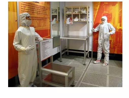
Chips are usually made in plants which are called as FABS. There are various precautions which have to be observed before making a chip. We know that chip’s are very small in size; hence production of each and every chip involves precision at atomic levels. Even very small particles like dust, hair etc. have the ability to ruin a chip and its performance. So the chip making process should be carried in a very clean room with specially made furniture and air circulation systems. The workers are given a special type of suit called ‘Bunny suit’ to prevent hair fall and other contaminations during chip manufacturing process.
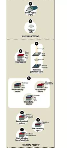
How to make a IC Chip?
Chips are usually made in plants which are called as FABS. There are various precautions which have to be observed before making a chip. We know that chip’s are very small in size; hence production of each and every chip involves precision at atomic levels. Even very small particles like dust, hair etc. have the ability to ruin a chip and its performance. So the chip making process should be carried in a very clean room with specially made furniture and air circulation systems. The workers are given a special type of suit called ‘Bunny suit’ to prevent hair fall and other contaminations during chip manufacturing process.
Chip Manufacturing is a very complex process as it involves very high level of precision. The following steps are involved in chip manufacturing process.
· The first step in the process of chip manufacturing is the melting and refining of sand to produce 99.9% pure silicon ingots. This process is done with the help of FABS.
· Then a SAW is used to cut the ingots into several wafers. They are cleaned thoroughly and multiple chips can be made from a single wafer.
· Now over the silicon wafer, a non-conducting layer of silicon-di-oxide is grown. Then a photosensitive chemical called photoresist is used to cover the layer of silicon-di-oxide.
· To harden the layer of silicon-di-oxide, it is subjected to ultraviolet radiation. The unexposed parts of the layers are etched away with the help of hot gases. The silicon base and silicon-di-oxide layer are further etched to varying depths. This process of hardening photoresist is called photolithography. Photolithography can be continued any number of times with different masks, so as to get a more complex design.
· The photoresist created using photolithography is then stripped away from the chip. The electrical conductivity of certain parts of the chip can be altered by doping chemicals along with heat and pressure.
· Now for creating conducting paths between the components, the chip is covered with a thin layer of aluminum and the lithography and etching process is done again to remove everything except the thin conducting pathways.
· After the completion of process, every chip is tested to analyze its performance. Good chips are separated from the wafer using a diamond saw and the bad chips which failed the tests are disposed.
To get a clear idea of the chip making process you can refer the diagram below