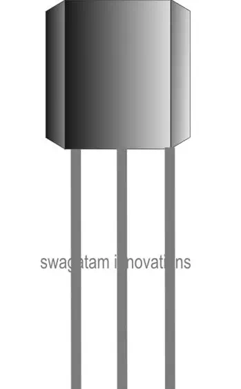
Hall Effect sensors are miniature SMD ICs based on CMOS technology which are able to convert fast switching magnetic fields induced over their surfaces into distinct and well defined logic outputs. A few of the major types of these sensors involving the respective output patterns are discussed here.
Technical Parameters
· Hall effect sensors are miniature monolithic CMOS ICs (Integrated Circuits) which are designed to sense changing magnetic fields at close proximities and toggle its output accordingly. The theory was fundamentally discovered by the scientist Edwin Herbert Hall way back in the year 1879.
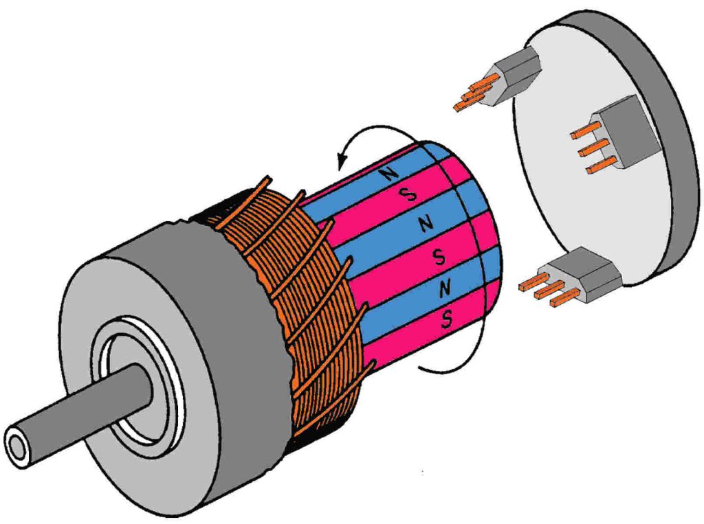
· The main areas of applications of these devices mostly include speed measurements as in speedometers, frequency meters, tachometers etc.
· A Hall effect sensor may primarily comprise of a temperature regulated Hall-plate along with a comparator stage, an active compensation network and an open drain output transistor.
· To make the IC sense a magnetic field, it becomes important that the magnetic lines of flux strike perpendicular to its surface and is not beyond 5mm from the IC.
· The above magnetic field is sensed by the Hall plate and a “Hall” voltage is developed across the biased Hall plate proportional to the induced magnetic flux. This voltage is compared with the internally set threshold of the IC in the comparator stage. If the applied magnetic flux is at optimal levels and exceeds the set threshold point, the open drain output transistor instantly switches, changes state and toggles the output.
· The IC also incorporates an internal hysteresis control stage which monitors the threshold transitions and makes sure the output does not oscillate during the transition points.
· Electronic devices usually may be quite prone to ambient temperature fluctuations which may drastically affect their output consistency. An internal temperature compensator inside Hall effect ICs is specially employed to tackle this problem. In case the ambient temperature tends to increase, the temperature-dependant bias stage raises the supply voltage of the Hall plate appropriately and compensates the falling induction of the magnetic field under the influence of high temperatures.

· An internal active offset compensation system ensures constant magnetic response characteristics of the IC irrespective of voltage and temperature fluctuations.
· All in all these ICs are reasonably robust by design and exhibit outstanding resistance against mechanical stresses.
Hall Efect Types – Switching Modes
Hall effect ICs typically come under the following major types, primarily depending upon their modes of switching:
· Sensors With Bipolar Switching Mode: In this type the IC shows distinct switching behavior for both the poles of the induced magnetic flux. With the South Pole directed towards the branded side of the IC, its output is switched low and with the North Pole applied to the branded side forces the IC’s output to go high. On complete removal of the applied magnetic field may cause the IC either to lose the switched instantaneous output state or retain it, the result may not be defined with ICs coming under the above type.
· Sensors With Unipolar Switching Mode: As the name suggests these sensors will respond particularly when a magnetic south pole is induced over its branded surface making its output immediately low, and, turning it high as soon as the induction is abandoned. The sensor won’t respond to the flipped side, that is to the North Pole of a magnet.
· Sensor With Unipolar Switching and Output Inverted: Here the basic nature of the sensor remains quite similar to the above type, however the output behavior exhibits exactly the opposite results with the respective inductions.
· Sensors With Latching Feature: Again the name refers to the specific nature that these particular types may own, the branded side when subjected to a magnetic South Pole switches its output high and switches back to low in response to a North Pole, however the removal of the magnetic fields does not inhibit the output from changing state, rather keeps it latched to the particular instantaneous level.
Typical Wiring Connection of a Hall Effect Sensor
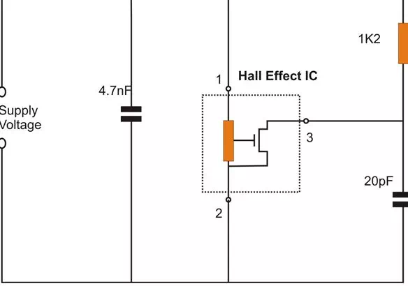
The diagram shown alongside illustrates how typical Hall effect sensors may be configured using a few external passive components. The specified components may be required to ensure added stabilization to the device and it’s functioning.


