The operation of an NPN transistor can be explained by having a look at the following figure, in which emitter-base junction is forward biased and collector-base junction is reverse biased.
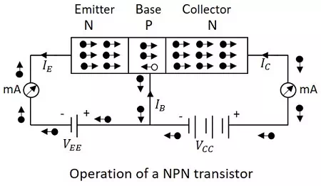
The voltage VEE provides a negative potential at the emitter which repels the electrons in the N-type material and these electrons cross the emitter-base junction, to reach the base region. There a very low percent of electrons recombine with free holes of P-region. This provides very low current which constitutes the base current IB. The remaining holes cross the collector-base junction, to constitute the collector current IC.
As an electron reaches out of the collector terminal, and enters the positive terminal of the battery, an electron from the negative terminal of the battery VEE enters the emitter region. This flow slowly increases and the electron current flows through the transistor.
Hence we can understand that −
- The conduction in a NPN transistor takes place through electrons.
- The collector current is higher than the emitter current.
- The increase or decrease in the emitter current affects the collector current.
Advantages
There are many advantages of a transistor such as −
- High voltage gain.
- Lower supply voltage is sufficient.
- Most suitable for low power applications.
- Smaller and lighter in weight.
- Mechanically stronger than vacuum tubes.
- No external heating required like vacuum tubes.
- Very suitable to integrate with resistors and diodes to produce ICs.
There are few disadvantages such as they cannot be used for high power applications due to lower power dissipation. They have lower input impedance and they are temperature dependent.