
A smartphone can contain a circuit board crowded with processors, memory chips, sensors, power regulators, antennas, and tiny resistors that are barely visible without magnification. A laptop, vehicle control unit, or medical monitor may be more complex still. Yet these boards are made repeatedly, at high speed, with remarkably consistent electrical connections.
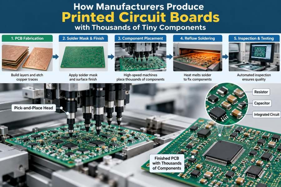
That consistency is not achieved by simply placing parts on a board. It comes from a chain of tightly controlled processes: translating an electrical design into copper patterns, building a layered board, applying solder paste with precision, placing components automatically, and inspecting every critical stage.
For electronics students, understanding this chain connects circuit diagrams to real hardware. For working engineers, it explains why seemingly small decisions about footprints, clearances, materials, or component packages can determine whether a design is easy to manufacture or unexpectedly difficult.
The finished printed circuit board, or PCB, looks like one object. In production, however, it is the result of two linked manufacturing worlds: bare-board fabrication and electronic assembly. Here is how thousands of tiny components become a functioning product.
🧩 The PCB Is More Than a Green Board
A PCB is a rigid, flexible, or rigid-flex insulating structure carrying conductive copper paths. Those paths replace much of the hand wiring that older electronic equipment required, while also controlling signal routes, power distribution, grounding, and component placement.
The familiar green color is usually solder mask, not the board material itself. Under it may be several copper layers separated by insulating dielectric material, most commonly fiberglass-reinforced epoxy in rigid boards.
A dense modern assembly may contain components on both sides, copper routing on many internal layers, and thousands of solder joints. The board has to deliver electrical connectivity, mechanical support, heat paths, and suitable electromagnetic behavior at the same time.
📐 A Schematic Must Become Manufacturable Data
Production begins long before a factory receives a panel. The design team creates a schematic that describes electrical intent, then a layout that places physical component footprints and routes copper traces between them.
Fabricators need layer images, drill information, board outlines, material requirements, and notes. Assemblers need a bill of materials, component placement coordinates, rotation conventions, assembly drawings, and instructions for any special processes.
Modern design tools export these data in standardized or widely used manufacturing formats. But exported files are not automatically error-free. A reversed polarity marker, mismatched footprint, or ambiguous coordinate origin can cause a costly production interruption.
🔍 Design for Manufacturability Starts at Layout
Design for manufacturability, often called DFM, means designing within the realistic capabilities and process limits of the intended supply chain. It is not a cosmetic final review; it affects the layout from the beginning.
Trace width and spacing, drill diameter, annular ring around a drilled hole, copper-to-edge clearance, and solder-mask openings must all be feasible for the selected board technology. Tighter features can be made, but they may increase cost, yield risk, or lead time.
Assembly has its own limits. Components need adequate space for pick-and-place nozzles, soldering, inspection, rework, and test access. A layout that is electrically correct but leaves no test pads or places a tall connector too close to a small component can be troublesome on the factory floor.
🧱 Choosing the Stackup and Base Material
The stackup is the sequence of copper and insulating layers through the board thickness. A simple board may have two copper layers. Dense digital, radio-frequency, power, and high-reliability products often use more layers to create dedicated ground planes, power planes, and controlled signal routing.
Rigid boards commonly use glass-fiber epoxy laminates. Flexible circuits use flexible polymer films, and metal-core boards may help transfer heat from LEDs or power devices. Material choice depends on operating temperature, mechanical needs, high-frequency loss, voltage isolation, thermal behavior, and cost.
Layer arrangement affects signal integrity. A fast signal routed close to a continuous reference plane has a predictable return-current path and more controllable impedance than one crossing gaps in a plane. This is why stackup is an electrical decision as well as a fabrication decision.
🧼 Preparing Copper-Clad Panels
Bare-board fabrication often starts with copper-clad laminate: an insulating panel covered with copper foil on one or both sides. Before imaging, the copper surface is cleaned so photoresist and later finishes adhere reliably.
Surface contamination from handling, oxidation, or processing residues can lead to incomplete pattern transfer or weak bonding. Manufacturers control cleaning chemistry, rinse quality, and handling because tiny defects can matter when trace geometries are small.
For multilayer boards, inner copper layers are patterned first. They will later be bonded inside the stack and cannot be visually inspected after lamination, so inspection at this stage is particularly valuable.
☀️ Imaging the Copper Circuit Pattern
To create traces and pads, the fabricator applies a light-sensitive material called photoresist. Artwork derived from the layout is aligned to the panel, and ultraviolet exposure changes selected areas of the resist.
After development, some regions are protected while others are exposed for chemical processing. In a subtractive process, unwanted copper is etched away, leaving the intended conductive pattern behind. The remaining resist is then removed.
Alignment matters on every layer. If an internal layer shifts relative to another, vias and pads may not line up as intended. Factories account for predictable material movement, but the design must still allow practical registration tolerances.
🔬 Etching Defines Traces, Pads, and Spacing
Etching removes copper chemically rather than cutting it mechanically. The process must remove unwanted copper thoroughly without excessively narrowing the protected traces. Fine features are sensitive to over-etching and variations in copper thickness.
Trace geometry is not always perfectly rectangular after etching; the sidewalls can taper. For ordinary circuits this may be unremarkable, but for fine-pitch designs, controlled-impedance routes, or high-current conductors, the finished geometry deserves attention.
After etching, automated optical inspection may compare the produced pattern with the intended data. It can identify opens, shorts, missing features, and certain pattern defects before a flawed layer is buried in a multilayer board.
🥪 Laminating Multilayer Boards
Multilayer construction combines etched inner layers with sheets of partially cured insulating resin, often called prepreg, and outer copper foils. Heat and pressure cure the resin and bond the stack into a solid panel.
This stage resembles making a carefully aligned composite sandwich, except each internal copper image must stay in registration while resin flows during pressing. Material movement, copper distribution, panel size, and press conditions can all influence the final result.
The reward is much greater routing density and better electrical control. The tradeoff is more process complexity: an internal defect or registration problem can make the complete panel unusable.
🕳️ Drilling Holes and Forming Vias
Drilled holes create mounting holes, connector holes, and vias: vertical electrical connections between copper layers. Mechanical drilling remains common, while lasers are used for very small blind microvias in high-density interconnect boards.
A through-hole via runs from the top to the bottom of the board. A blind via connects an outer layer to one or more internal layers, while a buried via exists only between internal layers. These structures can free routing space, but they raise fabrication complexity.
Drilling leaves debris and roughness inside the holes. The board goes through cleaning and desmear processes to prepare hole walls for reliable metallization. Poor preparation can weaken the electrical path later formed in the hole.
⚡ Plating Makes Holes Conductive
The insulating hole wall must become conductive before a via can connect layers. Manufacturers first deposit a very thin conductive seed layer through chemical processing, then build copper thickness using electroplating.
Plating also adds copper to outer-layer features. The resulting thickness must be sufficient for electrical reliability and for the mechanical stresses that occur as a board heats and cools during assembly and use.
Plated-through-hole quality is especially important in products exposed to temperature cycling. Different materials expand at different rates; repeated stress can challenge the copper barrel inside a hole if the design, materials, or plating process are unsuitable.
🎭 Outer-Layer Patterning Completes the Wiring
After drilling and plating, the outer layers receive their circuit patterns. Depending on the process flow, plating may build up intended conductors before unwanted copper is removed, helping define pads and traces.
At this point, the board’s copper network is substantially complete. It includes not only obvious signal traces but also ground areas, power distribution, thermal connections, shielding structures, fiducial marks, and test features.
Copper pours should not be treated as decorative empty-area fill. They influence heat spreading, return-current paths, etching balance, and board warpage. Their connection rules must match the circuit’s electrical purpose.
🎨 Solder Mask Protects and Guides Assembly
Solder mask is the insulating coating applied over most exposed copper. It helps prevent accidental solder bridges, protects copper from environmental exposure, and leaves only selected pads open for soldering.
Green is conventional, but mask can be many colors. Color itself is rarely the main engineering concern; contrast for inspection, process compatibility, and documentation are generally more useful considerations.
Mask openings must be designed carefully. If they are too small or misregistered, solderable pad area may be reduced. If adjacent openings merge where separation is needed, the risk of solder bridging can increase during reflow.
🏷️ Surface Finish Preserves Solderable Pads
Exposed copper oxidizes, so PCB fabricators apply a surface finish to pads that will later be soldered. Common choices include organic protective coatings, immersion tin, immersion silver, and nickel-gold-based finishes.
There is no universal best finish. Selection depends on storage conditions, component type, fine-pitch requirements, wire bonding or contact needs, cost, and the assembly process. A finish that works well for one product may be inappropriate for another.
For example, a fine-pitch package may need a very flat pad surface, while a board with edge contacts has different durability requirements. The finish should be specified as part of the manufacturing plan, not selected casually at the end.
✂️ Routing, V-Scoring, and Panelization
Factories usually process multiple boards together in a larger panel. Panelization improves machine handling and uses production area efficiently. Individual boards are separated later by routing, V-scoring, or tab routing.
V-scoring creates a controlled groove that allows boards to be snapped apart. Routed tabs leave small connection points that are cut or broken after assembly. The choice affects edge quality, nearby component clearance, panel strength, and depaneling stress.
Designers should keep vulnerable ceramic capacitors, connectors, and solder joints away from break lines. Mechanical bending during careless depaneling can crack parts or joints even if the board initially appears normal.
✅ Bare-Board Electrical Test Finds Opens and Shorts
Before assembly, many boards undergo electrical test to check that intended nets are connected and unintended nets are isolated. Fixtures with spring probes may contact dedicated test points; other systems use movable probes for lower-volume or more flexible testing.
This does not prove that every signal will meet its final high-speed or analog performance target. It verifies a foundational requirement: the fabricated copper connectivity is not obviously open or shorted.
Additional inspections may check hole quality, solder-mask registration, surface finish, dimensions, and layer alignment. The exact inspection plan depends on the board’s complexity, use case, and quality requirements.
📦 Components Arrive on Reels, Trays, and Tubes
Once bare boards are accepted, the assembly process begins. Surface-mount components commonly arrive in embossed tape on reels, ready for automated feeders. Larger or delicate parts may come in trays, while some through-hole components arrive in tubes or bulk packaging.
Incoming control matters because wrong values, wrong packages, moisture-sensitive parts, bent leads, counterfeit risk, and labeling mistakes can all affect production. A barcode system may link each reel or tray to the approved bill of materials and placement program.
Some packages absorb moisture from air. If they are heated rapidly in a reflow oven after unsuitable storage, internal moisture can cause package damage. Manufacturers follow component handling guidance and may bake parts when appropriate.
🧴 Stencil Printing Deposits Solder Paste
For surface-mount assembly, solder paste is printed onto the board’s pads. Solder paste is a controlled mixture of metal alloy particles and flux, a chemical system that helps clean surfaces and promote soldering during heating.
A thin metal stencil, laser-cut with openings matching the pad pattern, sits over the PCB. A squeegee pushes paste across it, depositing measured volumes through the openings. This is one of the most influential steps in the entire assembly line.
Too little paste can create weak or open joints. Too much can bridge neighboring pads. Aperture design, stencil thickness, board support, paste condition, print pressure, and cleaning all affect results.
📷 Solder Paste Inspection Catches Volume Errors Early
Many assembly lines inspect printed paste before components are placed. Two-dimensional systems check position and coverage; three-dimensional systems can estimate deposit height and volume.
Finding an error here is efficient because the board can often be cleaned and reprinted before valuable components are committed. Once parts are placed and soldered, diagnosis and rework become slower and riskier.
Inspection data can also reveal a developing process issue, such as a clogged stencil aperture or inadequate board support. In mature manufacturing, inspection is not just a pass/fail gate; it is feedback for process control.
🤖 Pick-and-Place Machines Populate Thousands of Parts
Pick-and-place machines use vacuum nozzles or specialized tooling to collect components from feeders, identify their orientation with cameras, and place them at programmed coordinates. Fast machines handle common small passive parts, while more flexible machines place connectors, large packages, and odd shapes.
A tiny resistor does not need an operator to align it by eye. The machine works from placement data, recognizes package features, compensates for measured position, and sets the part down onto paste-covered pads with controlled motion.
Speed is only one goal. Placement accuracy, feeder reliability, nozzle selection, component recognition, and correct rotation are equally significant. A board with thousands of parts makes even a low-frequency placement mistake costly if it is not detected quickly.
🧭 Fiducials Give Machines a Shared Reference
Fiducials are simple copper reference marks used by optical systems. Global fiducials help a machine locate the board, while local fiducials near fine-pitch devices can improve alignment where it matters most.
They are the manufacturing equivalent of registration marks on a printed page. Without clear, unobstructed fiducials, a machine may have difficulty correcting for small panel shifts, rotation, or dimensional variation.
Fiducial placement should be planned with solder mask, surface finish, rails, and component keep-outs in mind. A mark hidden by a fixture or placed too close to reflective copper features may be less useful than intended.
🔥 Reflow Ovens Turn Paste into Solder Joints
After placement, the board travels through a reflow oven with several temperature zones. The profile gradually heats the assembly, activates flux, melts the solder alloy, and then cools it at a controlled rate to form joints.
The thermal profile must suit the paste, board mass, package types, and component limits. Heating too aggressively can stress parts or create defects; insufficient heating can produce incomplete soldering. Large connectors and tiny chips on the same board make uniform heating harder.
When solder melts, surface tension can help draw properly aligned terminations toward their pads. This self-alignment effect is useful but limited. It cannot reliably rescue a seriously misplaced part, incorrect footprint, or badly imbalanced paste deposit.
🪞 Double-Sided Assembly Adds Process Decisions
Many products need components on both sides of the PCB. The first side is printed, populated, and reflowed; the board is then turned over for the second side. Whether this is straightforward depends on the component mix and process sequence.
Heavy parts on the first side may require special consideration during the second reflow. Thermal exposure also accumulates, so sensitive components, connectors, adhesives, or finishes may influence which side is assembled first.
Double-sided density saves area, but it complicates fixturing, inspection access, rework, and test. Engineers should not assume that unused space on the underside is free of manufacturing consequences.
🌊 Wave and Selective Soldering Serve Through-Hole Parts
Some connectors, transformers, switches, and power components use leads that pass through holes. They can be soldered manually in low-volume work, but volume production often uses wave soldering or selective soldering.
In wave soldering, the underside of a prepared board passes over a flowing wave of molten solder. Selective soldering directs soldering action to chosen locations, which is useful when mixed surface-mount and through-hole layouts would make a full wave risky.
Lead spacing, component orientation, solder thieves, thermal relief patterns, and keep-out areas all affect results. Mixed-technology boards benefit from early coordination between the layout engineer and the assembly process engineer.
🔎 Optical and X-Ray Inspection Look for Hidden Defects
Automated optical inspection, or AOI, uses cameras to check visible features such as component presence, polarity markings, alignment, solder bridges, and many types of insufficient or excessive solder.
Some joints cannot be adequately seen from above. Ball-grid-array packages, for example, have solder balls beneath the package body. X-ray inspection can reveal hidden solder connections, bridging, voiding patterns, and alignment issues, though interpretation requires trained judgment.
Neither method sees everything. Optical inspection can be confused by reflections or unusual component appearances, while X-ray images do not automatically establish every electrical or functional property. Inspection methods complement one another.
🧪 Testing Proves More Than Physical Appearance
A board can look well assembled and still contain a wrong value, damaged semiconductor, marginal solder connection, or programming error. Electrical testing adds another layer of evidence.
Common approaches include in-circuit test, which probes selected nodes; flying-probe test, which uses movable probes; boundary-scan methods supported by certain integrated circuits; and functional test, which powers the product and verifies intended behavior.
The best test strategy is designed into the product. Accessible test pads, isolation options, diagnostic firmware, and clear pass criteria reduce troubleshooting time. Adding test access after routing is complete is often far more difficult.
🛠️ Rework Is Valuable but Not a Substitute for Control
Defective assemblies can sometimes be repaired by removing and replacing components, adding solder, cleaning bridges, or correcting placement errors. Skilled rework is essential during prototyping and can recover otherwise valuable production boards.
However, repeated rework applies more heat and handling to pads, laminate, and nearby parts. It may hide a process problem rather than solve it. A rising rework rate is usually a signal to investigate stencil printing, placement, profiling, materials, or design details.
For fine-pitch and high-reliability products, rework procedures need suitable tools, inspection, and traceability. “It powers on” is not always sufficient evidence that a repaired joint will remain reliable in service.
📊 Yield, Traceability, and Process Feedback
Yield is the share of units that pass a defined manufacturing stage without unacceptable defects. Improving yield is not merely about rejecting fewer boards; it means learning where variation enters the process and preventing recurrence.
Factories collect data from printers, placement machines, ovens, inspection systems, and tests. Traceability may connect a finished board to its material lots, machine settings, operator actions, inspection images, and test record.
That record is especially useful when a field issue appears later. It helps engineers determine whether the problem is isolated, associated with a component lot, related to a process change, or rooted in the original design.
🌡️ Reliability Depends on the Product Environment
A board that works on a quiet laboratory bench may face vibration, temperature cycling, humidity, contamination, mechanical loading, or electrical transients in real service. Manufacturing quality must be considered alongside the actual environment.
Automotive, industrial, aerospace, consumer, and medical applications can impose very different qualification expectations. The appropriate design margins, materials, inspection depth, and documentation depend on the consequence of failure and the conditions of use.
Reliability is therefore a system property. Component selection, land pattern design, board stiffness, enclosure design, thermal paths, conformal coating where appropriate, and assembly quality all contribute.
⚠️ Common Design Choices That Create Factory Problems
Many assembly problems are preventable. They arise when a layout is completed in isolation from the physical processes that must print, place, heat, inspect, and test it.
- Unverified footprints: a pad pattern that does not match the actual package can cause poor joints or impossible placement.
- Missing polarity and pin-one cues: clear markings reduce the chance of reversed diodes, capacitors, LEDs, and integrated circuits.
- Insufficient component clearance: crowded parts can block nozzles, inspection cameras, probes, or rework tools.
- Vias too close to pads: uncovered vias can draw solder away through capillary action in some layouts.
- No panel and depaneling plan: edge features may be damaged if breakaway details are treated as an afterthought.
- Test considered too late: a lack of accessible nodes can turn a simple fault into a long debugging exercise.
🤝 Collaboration Between Designer and Manufacturer
The most reliable path to production is an early conversation with the chosen fabricator and assembler. Their capabilities, preferred materials, stencil guidance, panel constraints, and test options can inform choices before the layout becomes expensive to change.
This does not mean every design must use the loosest rules or the cheapest process. It means each constraint should be deliberate. A high-density wearable product may justify advanced interconnect features, while a rugged controller may prioritize larger spacing and repairability.
A design review should ask practical questions: Can every component be sourced in its specified package? Can the board be built, inspected, programmed, tested, separated, and serviced? If an answer is uncertain, the production package is not yet complete.
🧠 The Core Principle: Build Quality into Every Stage
Manufacturing a component-dense PCB is not one miraculous machine operation. It is a controlled sequence in which every stage protects the next: accurate design data enables clean copper features; reliable pads enable paste printing; consistent paste supports placement and reflow; inspection and test reveal variation before products leave the factory.
The central lesson is that manufacturability is part of engineering. Electrical performance, physical layout, material behavior, automated handling, thermal processing, and verification cannot be separated once a circuit moves from a screen into volume production.
When designers understand the factory’s constraints and manufacturers understand the design’s intent, thousands of microscopic connections can be produced as a repeatable system rather than a fragile collection of individual parts.
A successful PCB is designed not only to work electrically, but to be fabricated, assembled, inspected, tested, and used reliably in the real world. That is the discipline behind the compact electronics we depend on every day. 🔌🧠🏭