Properties:
· It is a 8-bit microprocessor
· Manufactured with N-MOS technology
· 40 pin IC package
· It has 16-bit address bus and thus has 216 = 64 KB addressing capability.
· Operate with 3 MHz single-phase clock
· +5 V single power supply
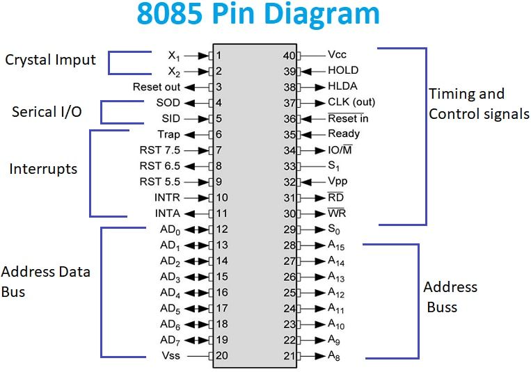
The logic pin layout and signal groups of the 8085nmicroprocessor are shown in Fig. 6. All the signals are classified into six groups:
· Address bus
· Data bus
· Control & status signals
· Power supply and frequency signals
· Externally initiated signals
· Serial I/O signals

Address and Data Buses:
· A8 – A15 (output, 3-state): Most significant eight bits of memory addresses and the eight bits of the I/O addresses. These lines enter into tri-state high impedance state during HOLD and HALT modes.
· AD0 – AD7 (input/output, 3-state): Lower significant bits of memory addresses and the eight bits of the I/O addresses during first clock cycle. Behaves as data bus during third and fourth clock cycle. These lines enter into tri-state high impedance state during HOLD and HALT modes.
Control & Status Signals:
· ALE: Address latch enable
· RD : Read control signal.
· WR : Write control signal.
· IO/M , S1 and S0 : Status signals.
Power Supply & Clock Frequency:
· Vcc: +5 V power supply
· Vss: Ground reference
· X1, X2: A crystal having frequency of 6 MHz is connected at these two pins
· CLK: Clock output
Externally Initiated and Interrupt Signals:
· RESET IN : When the signal on this pin is low, the PC is set to 0, the buses are tristated and the processor is reset.
· RESET OUT: This signal indicates that the processor is being reset. The signal can be used to reset other devices.
· READY: When this signal is low, the processor waits for an integral number of clock cycles until it goes high.
· HOLD: This signal indicates that a peripheral like DMA (direct memory access) controller is requesting the use of address and data bus.
· HLDA: This signal acknowledges the HOLD request.
· INTR: Interrupt request is a general-purpose interrupt.
· INTA : This is used to acknowledge an interrupt.
· RST 7.5, RST 6.5, RST 5,5 – restart interrupt: These are vectored interrupts and have highest priority than INTR interrupt.
· TRAP: This is a non-maskable interrupt and has the highest priority.
Serial I/O Signals:
· SID: Serial input signal. Bit on this line is loaded to D7 bit of register A using RIM instruction.
· SOD: Serial output signal. Output SOD is set or reset by using SIM instruction.


