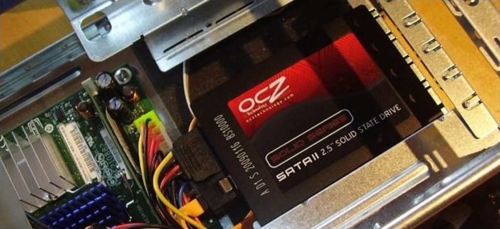
Solid-state drives (SSDs) are unanimously considered the enabling factor for bringing enterprise storage performances to the next level. Indeed, the rotating storage technology of Hard Disk Drives (HDDs) can’t achieve the access-time required by applications where response time is the critical factor. On the contrary, SSDs are based on solid state memories, namely NAND Flash memories: in this case, there aren’t any mechanical parts and random access to stored data can be much faster, thus addressing the above mentioned needs. In many applications though, the interface between host processors and drives remains the performance bottleneck. This is why SSD’s interface has evolved from legacy storage interfaces, such as SAS and SATA, to PCIe, which enables a direct connection of the SSD to the host processor. In this chapter we give an overview of the SSD’s architecture by describing the basic building blocks, such as the Flash controller, the Flash File System (FFS), and the most popular I/O interfaces (SAS, SATA and PCIe).
Introduction
Solid State Drives(SSDs) promise to greatly enhance enterprise storage performance. While electromechanical Hard Disk Drives (HDDs) have continuously ramped in capacity, the rotating-storage technology doesn’t provide the access-time or transfer rate performance required in demanding enterprise applications, including on-line transaction processing, data mining, and cloud computing. Client applications are also in need of an alternative to electromechanical disk drives that can deliver faster response times, use less power, and fit into smaller mobile form factors.
Flash-memory-based SSDs can offer much faster random access to data and faster transfer rates. Moreover, SSD’s capacity is now at the point where solid state drives can serve as rotating-disk replacements. But in many applications the interface between host and drives remains the performance bottleneck. SSDs with legacy storage interfaces, such as SAS and SATA, are proving useful, and PCI-Express (PCIe) SSDs will further increase performance and improve responsiveness, being directly connected to the host processor.
SSD’s Architecture
A basic block diagram of a solid state drive is shown in Fig. 1.1. In addition to memories and a Flash controller, there are usually other components. For instance, an external DC-DC converter can be added in order to drive the internal power supply, or a quartz can be used for a better clock precision. Of course, reasonable filter capacitors are inserted for stabilizing the power supply. It is also very common to have an array of temperature sensors for power management reasons. For data caching, a fast DDR memory is frequently used: during a write access, the cache

is used for storing data before their transfer to the Flash. The benefit is that data updating, e.g. of routing tables, is faster and does not wear out the Flash. A typical memory system is composed of several NAND memories [1]. Typically, an 8-bit bus [2, 3], usually called “channel”, is used to connect different memories to the controller (Fig. 1.1). It is important to underline that multiple Flash memories in a system are both a means for increasing storage density and read/write performances [4]. Operations on a channel can be interleaved, which means that a second chip can be addressed while the first one is still busy. For instance, a sequence of multiple write operations can be directed to a channel, addressing different NANDs, as shown in Fig. 1.2: in this way, the channel utilization is maximized by pipelining the data load phase. In fact, while the program operation takes place inside a memory chip, the corresponding Flash channel is free. The total number of Flash channels is a function of the target application, but tens of channels are becoming quite common. Thanks to interleaving, given the same Flash programming time, SSD’s throughput greatly improves. The memory controller is responsible for scheduling the accesses to the memory channels. The controller uses dedicated engines for the low level communication protocol with the Flash. Moreover, it is clear that the data load phase is not negligible compared to the program operation (the same comment is valid for data output): therefore, increasing I/O interface speed is another smart way to improve performances: DDR-like interfaces are discussed in more details in Chap. 2. As the speed increases, more NAND can be operated in parallel before saturating the channel. For instance, assuming a target of 30 MB/s, 2 NANDs are needed with a minimum DDR frequency of about 50 MHz. Given a page program time of 200 µs, at 50MHz four NANDs can operate in interleaved mode, doubling the write throughput. Of course, power consumption is another metric to be carefully considered. After this high level overview of the SSD’s architecture, let’s move to the heart of the architecture: the memory (Flash) controller.


