A normal P-N junction diode is usually fabricated by adjusting the P-type and N-type semiconductors on a single semiconductor crystal. The characteristics of a junction diode demonstrate that it is designed largely for operating in the forward direction. Applying a large amount of forward bias causes greater forward current with a small value of forward voltage.
However, reverse biasing the diode do not cause conduction of current till high values of reverse voltage are reached. If the reverse voltage is large enough, breakdown occurs and a reverse current starts to flow. Ordinary Junction diodes are generally damaged when this breakdown occurs. The flow of current in zener diodes is controlled by the minority charge carriers under the reverse bias condition, so they can also be referred to as break down diodes.

During specific conditions of fabrication, a special type of diode is formed that will not be ruined when the breakdown voltage is increased, given that the current does not exceed a defined limit to prevent the case of overheating. This type of devices is referred to as zener diodes.
Zener diodes are named after Clarence Melvin Zener by the Bell Laboratories, who discovered this type of electrical property. These diodes are a unique kind of diodes with heavy doping concentration at the time of fabrication. Due to the heavy doping, a large number of free electrons and electron holes are created and are responsible for conducting current due to minority carriers in reverse bias.
These diodes are designed to have avalanche characteristic that is very steep. Zener diodes are heavily doped silicon diodes, unlike normal diodes that exhibit an impulsive reverse break-down at comparatively low voltages.
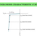
Zener diodes allow current to flow in the forward direction in the similar manner as an ideal diode, and also it permits current to flow in the reverse direction when the voltage is above a certain value known as the breakdown voltage. This voltage can also be referred as zener knee voltage or zener voltage.
If the voltage across the diode is increased, temperature increases and crystal ions vibrate with greater amplitude and all these leads to the breakdown of the depletion layer. When breakdown occurs, there will be a sharp increase in reverse current. A large amount of varying reverse current can pass through the diode without damaging it.
So zener diodes are intended to function in the reverse breakdown region with a reverse breakdown voltage (Vz) in the range 2.4 V to 200 V. The value of Vz depends on the doping concentration. When the Zener voltage is reached, the zener diode conducts current from its cathode terminal to its anode terminal.
The breakdown voltage or zener voltage across the zener diode fairly remains constant. The maximum amount of reverse current is limited by the wattage rating of the diode.
There are many different kinds of Zener diodes. They categorized by power dissipation, nominal working voltage, forward current, forward voltage, packaging type and maximum reverse current. General values for working zener knee voltage are 5.1 V, 6.2 V, 15 V and so on. Forward current can have a range from 200uA to 200A with the most common forward current being 10mA or 200mA.
Zener diodes found its use in several applications. They are widely used as voltage reference diodes in electronics circuits that allow simple and stable reference voltage regulator circuits to be prepared, as well as they are cheap and easy to manufacture.
They can be used as surge suppressors for device protection, in clipping circuits for clipping the waveforms that are not required, in different switching operations, as reference elements and they can be used to remove spikes that may damage a circuit or cause it to overload.
The unvarying reverse voltage of a zener diode renders it as a very useful component in controlling the output voltage against the variations in load resistance or variations in the input voltage provided from an unstable voltage source such as the battery bank of a renewable energy system which will fluctuate depending on the state of charge of the bank. The current through the Zener diode will change to keep the voltage within the adjustable threshold limits of zener action.
Manufacturers rate zener diodes according to their Vz value and the maximum power dissipation at room temperature i.e., 25ºC. This is an indication of the maximum reverse current that a zener diode can safely conduct electric current. Each zener knee voltage value is generally specified at lowest zener current. As a result the power dissipation values are used to indicate the safe operating range. Typical values of power dissipation ratings are from 150mW to 50W.
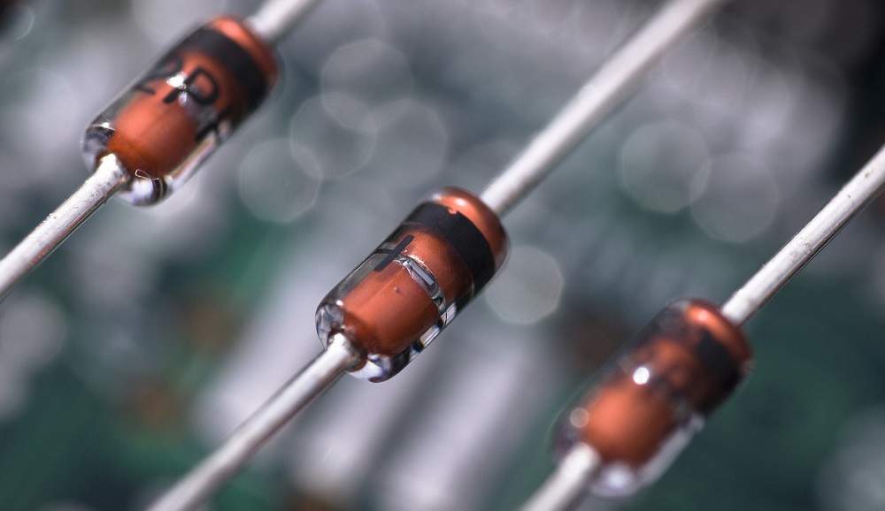
Zener diode can be identified by the terminal that is by observing a black color ring at cathode terminal. If the diode is an SMD component, then a colour band will be available for cathode terminal. By recognizing the zener diode code marked over the device, we can determine the value of it.