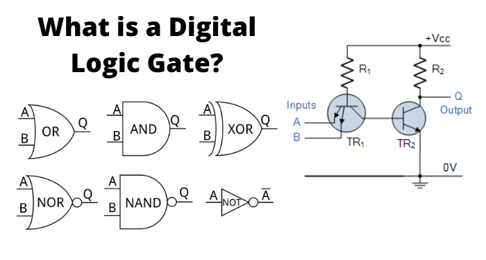
A Digital Logic Gate is an electronic circuit which makes logical decisions based on the combination of digital signals present on its inputs
Digital logic gates can have more than one input, for example, inputs A, B, C, D etc., but generally only have one digital output, (Q). Individual logic gates can be connected or cascaded together to form a logic gate function with any desired number of inputs, or to form combinational and sequential type circuits, or to produce differnt logic gate functions from standard gates.
Standard commercially available digital logic gates are available in two basic families or forms, TTL which stands for Transistor-Transistor Logic such as the 7400 series, and CMOS which stands for Complementary Metal-Oxide-Silicon which is the 4000 series of chips. This notation of TTL or CMOS refers to the logic technology used to manufacture the integrated circuit, (IC) or a “chip” as it is more commonly called.
Digital Logic Gate
Generally speaking, TTL logic IC’s use NPN and PNP type Bipolar Junction Transistors while CMOS logic IC’s use complementary MOSFET or JFET type Field Effect Transistors for both their input and output circuitry.
As well as TTL and CMOS technology, simple digital logic gates can also be made by connecting together diodes, transistors and resistors to produce RTL, Resistor-Transistor logic gates, DTL, Diode-Transistor logic gates or ECL, Emitter-Coupled logic gates but these are less common now compared to the popular CMOS family.
Integrated Circuits or IC’s as they are more commonly called, can be grouped together into families according to the number of transistors or “gates” that they contain. For example, a simple AND gate my contain only a few individual transistors, were as a more complex microprocessor may contain many thousands of individual transistor gates. Integrated circuits are categorised according to the number of logic gates or the complexity of the circuits within a single chip with the general classification for the number of individual gates given as:
Classification of Integrated Circuits
· Small Scale Integration or (SSI) – Contain up to 10 transistors or a few gates within a single package such as AND, OR, NOT gates.
· Medium Scale Integration or (MSI) – between 10 and 100 transistors or tens of gates within a single package and perform digital operations such as adders, decoders, counters, flip-flops and multiplexers.
· Large Scale Integration or (LSI) – between 100 and 1,000 transistors or hundreds of gates and perform specific digital operations such as I/O chips, memory, arithmetic and logic units.
· Very-Large Scale Integration or (VLSI) – between 1,000 and 10,000 transistors or thousands of gates and perform computational operations such as processors, large memory arrays and programmable logic devices.
· Super-Large Scale Integration or (SLSI) – between 10,000 and 100,000 transistors within a single package and perform computational operations such as microprocessor chips, micro-controllers, basic PICs and calculators.
· Ultra-Large Scale Integration or (ULSI) – more than 1 million transistors – the big boys that are used in computers CPUs, GPUs, video processors, micro-controllers, FPGAs and complex PICs.
While the “ultra large scale” ULSI classification is less well used, another level of integration which represents the complexity of the Integrated Circuit is known as the System-on-Chip or (SOC) for short. Here the individual components such as the microprocessor, memory, peripherals, I/O logic etc, are all produced on a single piece of silicon and which represents a whole electronic system within one single chip, literally putting the word “integrated” into integrated circuit.
These complete integrated chips which can contain up to 100 million individual silicon-CMOS transistor gates within one single package are generally used in mobile phones, digital cameras, micro-controllers, PIC’s and robotic type applications.
Moore’s Law
In 1965, Gordon Moore co-founder of the Intel corporation predicted that “The number of transistors and resistors on a single chip will double every 18 months” regarding the development of semiconductor gate technology. When Gordon Moore made his famous comment way back in 1965 there were approximately only 60 individual transistor gates on a single silicon chip or die.
The worlds first microprocessor in 1971 was the Intel 4004 that had a 4-bit data bus and contained about 2,300 transistors on a single chip, operating at about 600kHz. Today, the Intel Corporation have placed a staggering 1.2 Billion individual transistor gates onto its new Quad-core i7-2700K Sandy Bridge 64-bit microprocessor chip operating at nearly 4GHz, and the on-chip transistor count is still rising, as newer faster microprocessors and micro-controllers are developed.
Digital Logic States
The Digital Logic Gate is the basic building block from which all digital electronic circuits and microprocessor based systems are constructed from. Basic digital logic gates perform logical operations of AND, OR and NOT on binary numbers.
In digital logic design only two voltage levels or states are allowed and these states are generally referred to as Logic “1” and Logic “0”, or HIGH and LOW, or TRUE and FALSE. These two states are represented in Boolean Algebra and standard truth tables by the binary digits of “1” and “0” respectively.
A good example of a digital state is a simple light switch. The switch can be either “ON” or “OFF”, one state or the other, but not both at the same time. Then we can summarise the relationship between these various digital states as being:
| Boolean Algebra | Boolean Logic | Voltage State |
| Logic “1” | TRUE (T) | HIGH (H) |
| Logic “0” | FALSE (F) | LOW (L) |
Most digital logic gates and digital logic systems use “Positive logic”, in which a logic level “0” or “LOW” is represented by a zero voltage, 0v or ground and a logic level “1” or “HIGH” is represented by a higher voltage such as +5 volts, with the switching from one voltage level to the other, from either a logic level “0” to a “1” or a “1” to a “0” being made as quickly as possible to prevent any faulty operation of the logic circuit.
There also exists a complementary “Negative Logic” system in which the values and the rules of a logic “0” and a logic “1” are reversed but in this tutorial section about digital logic gates we shall only refer to the positive logic convention as it is the most commonly used.
In standard TTL (transistor-transistor logic) IC’s there is a pre-defined voltage range for the input and output voltage levels which define exactly what is a logic “1” level and what is a logic “0” level and these are shown below.
TTL Input & Output Voltage Levels
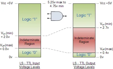
There are a large variety of logic gate types in both the bipolar 7400 and the CMOS 4000 families of digital logic gates such as 74Lxx, 74LSxx, 74ALSxx, 74HCxx, 74HCTxx, 74ACTxx etc, with each one having its own distinct advantages and disadvantages compared to the other. The exact switching voltage required to produce either a logic “0” or a logic “1” depends upon the specific logic group or family.
However, when using a standard +5 volt supply any TTL voltage input between 2.0v and 5v is considered to be a logic “1” or “HIGH” while any voltage input below 0.8v is recognised as a logic “0” or “LOW”. The voltage region in between these two voltage levels either as an input or as an output is called the Indeterminate Regionand operating within this region may cause the logic gate to produce a false output.
The CMOS 4000 logic family uses different levels of voltages compared to the TTL types as they are designed using field effect transistors, or FET’s. In CMOS technology a logic “1” level operates between 3.0 and 18 volts and a logic “0” level is below 1.5 volts. Then the following table shows the difference between the logic levels of traditional TTL and CMOS logic gates.
TTL and CMOS Logic Levels
| Device Type | Logic 0 | Logic 1 |
| TTL | 0 to 0.8v | 2.0 to 5v (VCC) |
| CMOS | 0 to 1.5v | 3.0 to 18v (VDD) |
Then from the above observations, we can define the ideal TTL digital logic gate as one that has a “LOW” level logic “0” of 0 volts (ground) and a “HIGH” level logic “1” of +5 volts and this can be demonstrated as:
Ideal TTL Digital Logic Gate Voltage Levels
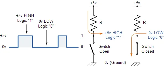
Where the opening or closing of the switch produces either a logic level “1” or a logic level “0” with the resistor R being known as a “pull-up” resistor.
Digital Logic Noise
However, between these defined HIGH and LOW values lies what is generally called a “no-man’s land” (the blue area’s above) and if we apply a signal voltage of a value within this no-man’s land area we do not know whether the logic gate will respond to it as a level “0” or as a level “1”, and the output will become unpredictable.
Noise is the name given to a random and unwanted voltage that is induced into electronic circuits by external interference, such as from nearby switches, power supply fluctuations or from wires and other conductors that pick-up stray electromagnetic radiation. Then in order for a logic gate not to be influence by noise in must have a certain amount of noise margin or noise immunity.
Digital Logic Gate Noise Immunity
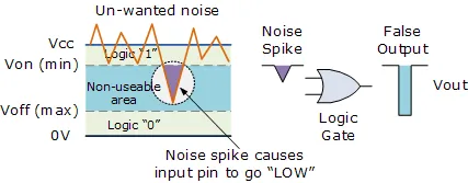
In the example above, the noise signal is superimposed onto the Vcc supply voltage and as long as it stays above the minimum level (VON(min)) the input an corresponding output of the logic gate are unaffected. But when the noise level becomes large enough and a noise spike causes the HIGH voltage level to drop below this minimum level, the logic gate may interpret this spike as a LOW level input and switch the output accordingly producing a false output switching. Then in order for the logic gate not to be affected by noise it must be able to tolerate a certain amount of unwanted noise on its input without changing the state of its output.
Simple Basic Digital Logic Gates
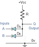
Simple digital logic gates can be made by combining transistors, diodes and resistors with a simple example of a Diode-Resistor Logic (DRL) AND gate and a Diode-Transistor Logic (DTL) NAND gate given below.
| Diode-Resistor Circuit | Diode-Transistor circuit |
 2-input AND Gate 2-input AND Gate | 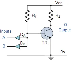 2-input NAND Gate 2-input NAND Gate |
The simple 2-input Diode-Resistor AND gate can be converted into a NAND gate by the addition of a single transistor inverting (NOT) stage. Using discrete components such as diodes, resistors and transistors to make digital logic gate circuits are not used in practical commercially available logic IC’s as these circuits suffer from propagation delay or gate delay and also power loss due to the pull-up resistors.
Another disadvantage of diode-resistor logic is that there is no “Fan-out” facility which is the ability of a single output to drive many inputs of the next stages. Also this type of design does not turn fully “OFF” as a Logic “0” produces an output voltage of 0.6v (diode voltage drop), so the following TTL and CMOS circuit designs are used instead.
Basic TTL Logic Gates
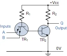
The simple Diode-Resistor AND gate above uses separate diodes for its inputs, one for each input. As a transistor is made up off two diode circuits connected together representing an NPN or a PNP device, the input diodes of the DTL circuit can be replaced by one single NPN transistor with multiple emitter inputs as shown.
2-input NAND Gate
As the NAND gate contains a single stage inverting NPN transistor circuit (TR2) an output logic level “1” at Q is only present when both the emitters of TR1 are connected to logic level “0” or ground allowing base current to pass through the PN junctions of the emitter and not the collector. The multiple emitters of TR1 are connected as inputs thus producing a NAND gate function.
In standard TTL logic gates, the transistors operate either completely in the “cut off” region, or else completely in the saturated region, Transistor as a Switch type operation.
Emitter-Coupled Digital Logic Gate
Emitter Coupled Logic or ECL is another type of digital logic gate that uses bipolar transistor logic where the transistors are not operated in the saturation region, as they are with the standard TTL digital logic gate. Instead the input and output circuits are push-pull connected transistors with the supply voltage negative with respect to ground.
This has the effect of increasing the speed of operation of the emitter coupled logic gates up to the Gigahertz range compared with the standard TTL types, but noise has a greater effect in ECL logic, because the unsaturated transistors operate within their active region and amplify as well as switch signals.
The “74” Sub-families of Integrated Circuits
With improvements in the circuit design to take account of propagation delays, current consumption, fan-in and fan-out requirements etc, this type of TTL bipolar transistor technology forms the basis of the prefixed “74” family of digital logic IC’s, such as the “7400” Quad 2-input NAND gate, or the “7402” Quad 2-input NORgate, etc.
Sub-families of the 74xxx series IC’s are available relating to the different technologies used to fabricate the gates and they are denoted by the letters in between the 74 designation and the device number. There are a number of TTL sub-families available that provide a wide range of switching speeds and power consumption such as the 74L00 or 74ALS00 NAND gate, were the “L” stands for “Low-power TTL” and the “ALS” stands for “Advanced Low-power Schottky TTL” and these are listed below.
• 74xx or 74Nxx: Standard TTL – These devices are the original TTL family of logic gates introduced in the early 70’s. They have a propagation delay of about 10ns and a power consumption of about 10mW. Supply voltage range: 4.75 to 5.25 volts
• 74Lxx: Low Power TTL – Power consumption was improved over standard types by increasing the number of internal resistances but at the cost of a reduction in switching speed. Supply voltage range: 4.75 to 5.25 volts
• 74Hxx: High Speed TTL – Switching speed was improved by reducing the number of internal resistances. This also increased the power consumption. Supply voltage range: 4.75 to 5.25 volts
• 74Sxx: Schottky TTL – Schottky technology is used to improve input impedance, switching speed and power consumption (2mW) compared to the 74Lxx and 74Hxx types. Supply voltage range: 4.75 to 5.25 volts
• 74LSxx: Low Power Schottky TTL – Same as 74Sxx types but with increased internal resistances to improve power consumption. Supply voltage range: 4.75 to 5.25 volts
• 74ASxx: Advanced Schottky TTL – Improved design over 74Sxx Schottky types optimised to increase switching speed at the expense of power consumption of about 22mW. Supply voltage range: 4.5 to 5.5 volts
• 74ALSxx: Advanced Low Power Schottky TTL – Lower power consumption of about 1mW and higher switching speed of 4nS compared to 74LSxx types. Supply voltage range: 4.5 to 5.5 volts
• 74HCxx: High Speed CMOS – CMOS technology and transistors to reduce power consumption of less than 1uA with CMOS compatible inputs. Supply voltage range: 4.5 to 5.5 volts
• 74HCTxx: High Speed CMOS – CMOS technology and transistors to reduce power consumption of less than 1uA but has increased propagation delay of about 16nS due to the TTL compatible inputs. Supply voltage range: 4.5 to 5.5 volts
Basic CMOS Digital Logic Gate
One of the main disadvantages with the TTL digital logic gate series is that the logic gates are based on bipolar transistor logic technology and as transistors are current operated devices, they consume large amounts of power from a fixed +5 volt power supply.
Also, TTL bipolar transistor gates have a limited operating speed when switching from an “OFF” state to an “ON” state and vice-versa called the “gate” or “propagation delay”. To overcome these limitations complementary MOS called “CMOS” (Complementary Metal Oxide Semiconductor) logic gates which use “Field Effect Transistors” or FET’s were developed.
As these gates use both P-channel and N-channel MOSFET’s as their input device, at quiescent conditions with no switching, the power consumption of CMOS gates is almost zero, (1 to 2μA) making them ideal for use in low-power battery circuits and with switching speeds upwards of 100MHz for use in high frequency timing and computer circuits.
2-input NAND Gate
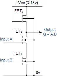
This CMOS gate example contains three N-channel MOSFET’s, one for each input FET1 and FET2 and one for the output FET3. When both the inputs Aand B are at logic level “0”, FET1 and FET2 are both switched “OFF” giving an output logic “1” from the source of FET3.
When one or both of the inputs are at logic level “1” current flows through the corresponding FET giving an output state at Q equivalent to logic “0”, thus producing a NAND gate function.
Improvements in the circuit design with regards to switching speed, low power consumption and improved propagation delays has resulted in the standard CMOS 4000 “CD” family of logic IC’s being developed that complement the TTL range.
As with the standard TTL digital logic gates, all the major digital logic gates and devices are available in the CMOS package such as the CD4011, a Quad 2-input NAND gate, or the CD4001, a Quad 2-input NOR gate along with all their sub-families.
Like TTL logic, complementary MOS (CMOS) circuits take advantage of the fact that both N-channel and P-channel devices can be fabricated together on the same substrate material to form various logic functions.
One of the main disadvantage with the CMOS range of IC’s compared to their equivalent TTL types is that they are easily damaged by static electricity. Also unlike TTL logic gates that operate on single +5V voltages for both their input and output levels, CMOS digital logic gates operate on a single supply voltage of between +3 and +18 volts.
Common CMOS Sub-families include:
• 4000B Series: Standard CMOS – These devices are the original Buffered CMOS family of logic gates introduced in the early 70’s and operate from a supply voltage of 3.0 to 18v d.c.
• 74C Series: 5v CMOS – These devices are pin-compatible with standard 5v TTL devices as their logic switching is implemented in CMOS but with TTL-compatible inputs. They operate from a supply voltage of 3.0 to 18v d.c.
Note that CMOS logic gates and devices are static sensitive, so always take the appropriate precautions of working on antistatic mats or grounded workbenches, wearing an antistatic wristband and not removing a part from its antistatic packaging until required.
