A memory controller has two fundamental tasks:
1. provide the most suitable interface and protocol towards both the host and the Flash memories;
2. efficiently handle data, maximizing transfer speed, data integrity and retention of the stored information.
In order to carry out such tasks, an application specific device is designed, embedding a standard processor—usually 8–16 bits—together with dedicated hardware to handle time-critical tasks.
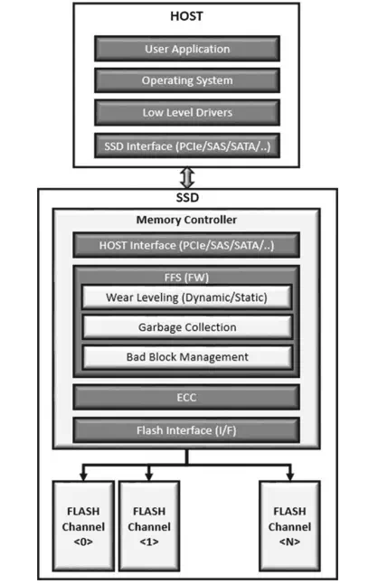
Generally speaking, the memory controller can be divided into four parts, which are implemented either in hardware or in firmware (Fig. 1.3).
Moving from the host to the Flash, the first part is the host interface, which implements the required industry-standard protocol (PCIe, SAS, SATA, etc.), thus ensuring both logical and electrical interoperability between SSDs and hosts. This block is a mix of hardware (buffers, drivers, etc.) and firmware, which decodes the command sequence invoked by the host and handles the data flow to/from the Flash memories.
The second part is the Flash File System (FFS) [5]: that is, the file system which enables the use of SSDs like magnetic disks. For instance, sequential memory access on a multitude of sub-sectors which constitute a file is organized by linked lists (stored on the SSD itself), which are used by the host to build the File Allocation Table (FAT). The FFS is usually implemented in form of firmware inside the controller, each sub-layer performing a specific function. The main functions are: Wear leveling Management, Garbage Collection and Bad Block Management. For all these functions, tables are widely used in order to map sectors and pages from the logical domain to the physical domain (Flash Translation Layer or FTL) [6, 7], as shown in Fig. 1.4. The top row is the logical view of the memory, while the bottom row is the physical one. From the host perspective, data are transparently written and overwritten inside a given logical sector: due to Flash limitations, overwrite on the same page is not possible; therefore, a new page (sector) must be allocated in the physical block, and the previous one is marked as invalid. It is clear that, at some point in time, the current physical block becomes full and a second one (coming from the pool of “buffer” blocks) has to take over that logic address.
The required translation tables are stored on the SSD itself, thus reducing the overall storage capacity.
Wear Levelling
Usually, not all the data stored within the same memory location change with the same frequency: some data are often updated while others don’t change for a very

Fig. 1.3 High level view of a Flash controller

long time—in the extreme case, for the whole life of the device. It’s clear that the blocks containing frequently-updated information are stressed with a larger number of write/erase cycles, while the blocks containing information updated very rarely are much less stressed.
In order to mitigate disturbs, it is important to keep the aging of each page/block as minimum and as uniform as possible: that is, the number of both read and program cycles applied to each page must be monitored. Furthermore, the maximum number of allowed program/erase cycles for a block (i.e. its endurance) should be considered: in case SLC NAND memories are used, this number is in the order of 20–30 k cycles, which is reduced to 10–15 k and 1–5 k for MLC and TLC NAND, respectively.
Wear Levelling techniques exploit the concept of logical to physical translation: each time the host application needs to update the same (logical) sector, the memory controller dynamically maps that sector to a different (physical) sector, of course keeping track of the mapping. The out-of-date copy of the sector is tagged as invalid and eligible for erase. In this way, all the physical blocks are evenly used, thus keeping the aging under a reasonable value.
Two kinds of approaches are possible: Dynamic Wear Levelling is normally used to follow up a user’s request of update, writing to the first available erased block with the lowest erase count; with Static Wear Levelling every block, even the least modified, is eligible for re-mapping as soon as its aging deviates from the average value.


