Processor vendors have continued to ramp the performance of individual processor cores, to combine multiple cores in one chip, and to develop technologies that can closely couple multiple chips in multi-processor systems. Ultimately, all of the cores in such a scenario need access to the same storage subsystem.


Enterprise IT managers are eager to utilize the multiprocessor systems because they have the potential of boosting the number of I/O operations per second (IOPS) that a system can process and also the number of IOPS per Watt. This multiprocessing computing capability offers better IOPS relative to cost and power consumption—assuming the processing elements can get access to the data in a timely fashion. Active processors waiting on data waste time and money.
There are, of course, multiple levels of storage technology in a system that ultimately feed code and data to each processor core. Generally, each core includes local cache memory that operates at core speed. Multiple cores in a chip share a second- level and, sometimes, a third-level cache. And DRAM feeds the caches. DRAM and caches access-times, together with data-transfer speed have scaled to match processor’s performance. The issue is the performance gap between DRAM and HDD in terms of access time and data rate. Disk/drive vendors have done a great job at designing and manufacturing higher-capacity, lower-cost-per-Gbyte disks/drives; but the drives inherently have limitations in terms of how fast they can access data, and then how fast they can transfer these data to DRAM. Access time depends on how quickly a hard drive can move the read head over the required data track on a disk, and the rotational latency of the addressed sector to move underneath the head.
The maximum transfer rate is dictated by the rotational speed of the disk and the data encoding scheme: together they determine the number of bytes per second that can be read from the disk. Hard drives perform relatively well in reading and transferring sequential data. But random seek operations add latency. And even sequential read operations can’t match the data appetite of the latest processors.
Meanwhile, enterprise systems that perform on-line transaction processing, such as financial transactions and data mining (e.g. applications for customer relationship management) require highly random access to data. Also cloud computing has strong random requirements, especially when looking at virtualization, which expands the scope of different applications that a single system has active at any one time. Every microsecond of latency directly relates to money, utilization of processors and system power.
Fortunately, Flash memories can help reducing the performance gap between DRAM and HDD. Flash is slower than DRAM but offers a lower cost per Gbyte of storage. That cost is more expensive than disk storage, but enterprises will gladly pay the premium because Flash also offers much better throughput in terms of Mbyte/s and faster access to random data, resulting in better cost-per-IOPS compared to rotating storage.
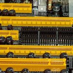
Neither the legacy disk-drive form factor nor the interface is ideal for Flash-based storage. SSD manufacturers can pack enough Flash devices in a 2.5-in form factor to easily exceed the power profile developed for disk drives. And Flash can support higher data transfer rates than even the latest generation of disk interfaces.
Let’s examine the disk interfaces more closely (Fig. 1.11). The third-generation SATA and SAS support 600 Mbyte/s throughput, and drives based on those interfaces have already found usage in enterprise systems. While those data rates support the

fastest electromechanical drives, new NAND Flash architectures and multi-die Flash packaging deliver aggregate Flash bandwidth that exceeds the throughput capabilities of SATA and SAS interconnects. In short, the SSD performance bottleneck has shifted from the storage media to the host interface. Therefore, many applications need a faster host interconnect to take full advantage of Flash storage.
The PCIe host interface can overcome this storage performance bottleneck and deliver unparalleled performance by attaching the SSD directly to the PCIe host bus. For example, a 4-lane (x4) PCIe Generation 3 (Gen3) link can deliver 4 GByte/s data rates. Simply put, PCIe meets the desired storage bandwidth. Moreover, the direct PCIe connection can reduce system power and slash the latency that’s attributable to the legacy storage infrastructure.
Clearly, an interface such as PCIe can handle the bandwidth of a multi-channel Flash storage subsystem and can offer additional performance advantages. SSDs that use a disk interface also suffer latency added by a storage-controller IC that handles disk I/O. PCIe devices connect directly to the host bus, thus eliminating the architectural layer associated with the legacy storage infrastructure. The compelling performance of PCIe SSDs has resulted in system manufacturers placing PCIe drives in servers as well as in storage arrays to build tiered storage systems that accelerate applications while improving cost-per-IOPS.
The benefits of using PCIe as a storage interconnect are clear. You can achieve over 6x the data throughput compared to SATA or SAS. You can eliminate components such as host bus adapters and SerDes ICs on the SATA and SAS interfaces—saving money and power at the system level. And PCIe moves the storage closer to the host CPU reducing latency, as shown in Fig. 1.12.
Latency, IOPS, bandwidth, power, interface speed, number of channels, NANDtype (SLC, MLC, TLC, QLC) are all parameters that SSD designers need to take into account to meet their target specifications at minimum cost. Looking forward,

emerging memories will be part of the game too. It is clear that, given this number of variables, a simple approach based on hardware prototyping is hard to pursue, especially when looking at the time-to-market.