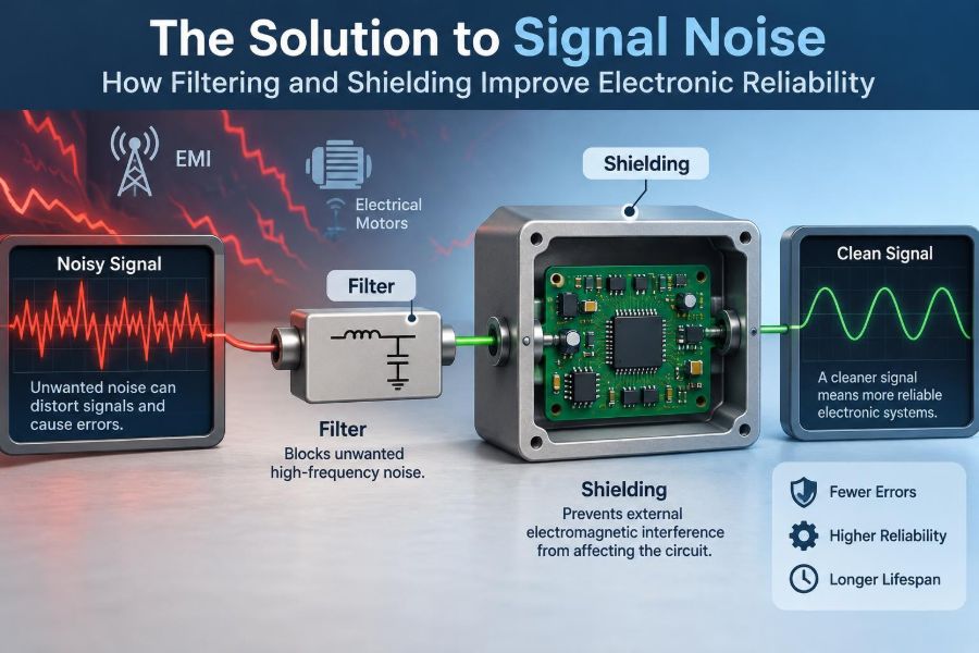

A smartphone drops a call beside a poorly routed charger cable. A medical sensor produces an occasional impossible reading. A microcontroller resets only when a motor starts. These failures can look random, which makes them among the most frustrating problems in electronics.
Often, the circuit is not “broken” in the usual sense. It is reacting to unwanted electrical energy that has entered through a power line, a signal wire, the air, or even the circuit board itself. That unwanted energy is broadly called noise.
Noise is not limited to advanced radio systems. It affects audio equipment, industrial controls, vehicle electronics, home appliances, embedded devices, and high-speed digital products. As systems use lower voltages, faster edges, and denser layouts, their tolerance for disturbance can shrink.
Filtering and shielding are two of the most useful ways to manage the problem. One removes or redirects unwanted frequency content; the other limits how effectively noise can enter or leave a system. Used thoughtfully, they turn a temperamental circuit into a dependable one.
📡 What Signal Noise Actually Means
In engineering, noise is any unwanted electrical variation that interferes with information or normal circuit operation. It may appear as a voltage ripple, a brief spike, a changing magnetic field, an unwanted current, or a radio-frequency signal.
The key word is unwanted. A 1 kHz sine wave is a useful audio signal in one circuit and interference in another. Whether something is noise depends on the function of the circuit receiving it.
Noise can reduce measurement accuracy, corrupt digital data, create audible hum, disturb wireless reception, or cause a control system to behave unpredictably. Its effect depends on amplitude, frequency, duration, coupling path, and receiver sensitivity.
🧭 The Three Parts of Every Noise Problem
Most electromagnetic interference problems can be understood through three elements: a source, a coupling path, and a victim. The source produces disturbance, the path carries it, and the victim responds badly to it.
A switching regulator, for example, can be the source. A nearby cable or shared ground connection can be the path. A sensitive analog-to-digital converter can be the victim.
This model prevents a common mistake: treating every problem only at the victim. A robust solution may instead reduce noise at its source or break the path that connects source and receiver.
⚡ Common Sources Inside Electronic Products
Many noise sources are created by the product itself. Fast switching currents are particularly significant because a rapid current change creates voltage disturbances across unavoidable resistance and inductance.
- Switch-mode power supplies and DC-DC converters
- Clock lines, memory buses, and fast digital interfaces
- Motors, relays, solenoids, and their switching contacts
- LED drivers, inverters, and pulse-width-modulated loads
- Electrostatic discharge from people and connectors
A relay coil may be harmless while energized, yet generate a substantial transient when switched off. A flyback diode or other suppression network is therefore not an optional afterthought; it controls energy stored in the coil.
🌐 Noise from the Outside World
External interference can arrive from nearby equipment, radio transmitters, mains wiring, lightning-related surges, and electrostatic events. A product does not need to contain a radio receiver to be affected by radio-frequency energy.
Long cables are especially vulnerable because they can behave like antennas. An industrial sensor cable routed beside a motor drive may pick up common-mode interference even if the sensor signal itself changes very slowly.
The operating environment matters. A circuit that works perfectly on an uncluttered bench may face much harsher electrical conditions in a factory, vehicle, hospital, or telecommunications installation.
🪢 Conducted Noise and Radiated Noise
Conducted noise travels through a physical electrical connection, such as a power lead, ground conductor, signal cable, or shared supply impedance. Supply ripple entering an analog amplifier through its power pins is a typical example.
Radiated noise travels through electric or magnetic fields without requiring a direct conductive connection. A loop of wire near a transformer can pick up a changing magnetic field, while a poorly contained clock signal can radiate outward.
| Noise route | Typical example | Common first response |
|---|---|---|
| Conducted | Switching ripple on a DC supply | Decoupling, filtering, impedance control |
| Capacitive coupling | Fast voltage line disturbing a high-impedance input | Spacing, grounding, shielding |
| Inductive coupling | Motor current affecting a sensor loop | Reduce loop area, twist pair, separate routing |
| Radiated RF | Wireless transmitter affecting circuitry | Enclosure shielding, filtered entry points |
🔄 Differential Noise and Common-Mode Noise
Differential noise appears between two conductors that carry a signal. It directly competes with the intended signal, which is why it can be troublesome in low-level analog measurements.
Common-mode noise appears similarly on both conductors relative to a reference such as chassis or earth. A balanced receiver can reject much of it if the pair is well matched, but cable imbalance and poor layout can convert it into differential noise.
This distinction guides component selection. A differential filter acts between signal conductors, while a common-mode choke is designed to impede unwanted current flowing in the same direction on both conductors.
🎵 Frequency Determines the Right Response
Noise is not one uniform phenomenon. A slow 50 or 60 Hz hum, a converter’s switching ripple, and a short nanosecond-scale edge occupy very different frequency ranges and need different treatments.
Every filter has a frequency-dependent response. A capacitor that works well at low frequencies may become less effective at high frequencies because its leads and internal construction add inductance. Similarly, an inductor may lose useful impedance as frequency rises.
Before adding parts, ask: what frequency content is causing the failure? A spectrum analyzer, oscilloscope with appropriate probing, or even a carefully designed test can reveal more than repeated component swapping.
🧱 Impedance Is the Practical Language of Filtering
Filtering works by giving unwanted energy a less favorable path while preserving the wanted signal. That behavior is described by impedance, the opposition a circuit presents to alternating current.
Capacitors generally present lower impedance as frequency increases, so they can divert high-frequency noise to a reference plane. Inductors generally present higher impedance as frequency increases, so they can impede high-frequency noise in a series path.
Neither statement is absolute at all frequencies. Real components have parasitic resistance, capacitance, and inductance. Effective design uses real part data and recognizes where a component stops behaving like its ideal schematic symbol.
🔽 Low-Pass Filters for Cleaner Measurements
A low-pass filter passes slow or low-frequency signals while attenuating higher-frequency content. It is common at sensor inputs, audio paths, reference voltages, and analog-to-digital converter inputs.
Suppose a temperature sensor changes only over seconds, but the cable picks up fast switching noise. A modest low-pass filter can preserve the temperature information while reducing the unwanted fluctuations before conversion.
The trade-off is response time. Too low a cutoff frequency makes a system sluggish, and excessive filtering can distort a legitimate rapidly changing signal. The desired bandwidth should be chosen from the application, not guessed from a convenient capacitor value.
🔼 High-Pass Filters and AC Coupling
A high-pass filter blocks DC and slow variations while allowing faster changes to pass. AC coupling capacitors in audio circuits are familiar examples: they remove a DC offset between stages without removing the audible content.
High-pass behavior can also suppress slow baseline drift or low-frequency interference. However, it will not solve every noise issue. If a signal itself contains low-frequency information, an aggressive high-pass filter removes useful data along with the disturbance.
At power-up, coupling capacitors can create settling effects. Designers should consider startup behavior, input bias currents, and overload recovery rather than evaluating only steady-state waveforms.
🎚️ Band-Pass and Notch Filtering
A band-pass filter retains a chosen frequency range and suppresses frequencies above and below it. Radio receivers and vibration-monitoring systems use this principle when the desired information occupies a defined band.
A notch filter does the opposite at one narrow region: it rejects a troublesome frequency while passing much of the surrounding spectrum. Removing mains-frequency hum from a measurement is a familiar use case.
Notch filters require care. Their component tolerances, temperature drift, and phase response can matter, and a notch near useful signal content may produce misleading results. Digital post-processing can sometimes help, but it cannot recover information already lost to front-end overload.
🧲 Ferrite Beads and Common-Mode Chokes
Ferrite components are widely used because their impedance can rise strongly over a selected high-frequency range. A ferrite bead placed in series with a supply line can reduce high-frequency current traveling between noisy and sensitive areas.
A common-mode choke contains coupled windings arranged so normal differential current largely passes while common-mode current encounters substantial impedance. It is useful on cable interfaces, power entries, and balanced signal lines.
These parts are not universal cures. DC bias can alter the behavior of some ferrite materials, and saturation or excessive current can reduce an inductor’s effectiveness. Select parts using impedance-versus-frequency and current information rather than their appearance alone.
🔋 Decoupling Capacitors at Power Pins
A decoupling capacitor supplies brief local current when an integrated circuit switches and reduces the need for that current to travel through a long, inductive power path. It also helps prevent one circuit block from injecting disturbances into another through the supply network.
Placement is crucial. A small capacitor placed close to an IC’s power and ground pins is usually more valuable at high frequency than a larger capacitor placed several centimeters away.
Decoupling is not simply a matter of scattering capacitors across a board. The current loop includes the capacitor, vias, traces, planes, and IC pins. A compact loop and a continuous reference plane reduce inductance and improve performance.
🏦 Bulk Capacitors and Energy Storage
Bulk capacitance handles lower-frequency load changes and provides stored energy over longer intervals than small ceramic decouplers. It can support a supply when a motor starts, a radio transmits, or a processor changes operating mode.
Its equivalent series resistance and inductance matter. A large electrolytic capacitor may store useful energy but respond poorly to a very fast transient, so it is commonly paired with smaller capacitors that handle higher frequencies.
More capacitance is not automatically safer. Inrush current, regulator stability, physical size, cost, and component lifetime all influence the correct choice.
📐 LC and Pi Filters on Power Rails
An LC filter combines an inductor and capacitor to attenuate ripple more strongly than either component alone over an intended range. A pi filter commonly uses capacitor-inductor-capacitor topology, resembling the Greek letter π in a schematic.
These filters are useful when a noisy supply must feed a sensitive analog section. For example, a digital converter rail may need separation from a precision reference or low-noise amplifier supply.
They can also resonate. A filter interacting with a switching regulator’s control loop may amplify a frequency region or affect regulator stability. Damping, component parasitics, and the regulator manufacturer’s design guidance all deserve attention.
🧪 Analog Inputs Need Protection Before Precision
A high-resolution measurement system cannot recover accuracy if interference drives its input amplifier or converter beyond its valid range. Input protection, filtering, and sensible gain staging should come before attempts to refine software calculations.
Series resistance can limit fault and transient current. Capacitors can reduce bandwidth. Clamp structures may protect against voltage excursions, but their leakage, capacitance, and behavior during repeated events must suit the measurement requirement.
For very small signals, the filter’s own noise and resistor thermal noise may be relevant. Design is always a balance between protection, bandwidth, source impedance, accuracy, and recovery time.
🧠 Digital Circuits Are Not Immune
Digital logic interprets voltages as discrete states, but the physical signals are analog waveforms with finite rise times. A noisy threshold crossing can cause extra transitions, timing uncertainty, false interrupts, or corrupted communication.
Fast edges contain high-frequency energy even when the clock rate appears modest. A microcontroller running at a moderate frequency can still create significant emissions if its outputs switch sharply and the return current path is poorly controlled.
Schmitt-trigger inputs, debouncing, series termination, and adequate power integrity can improve resilience. They should be selected based on the actual interface rather than applied blindly to every line.
🧾 Signal Integrity and EMI Are Connected
Signal integrity concerns whether a waveform arrives at its receiver with acceptable timing and voltage shape. Electromagnetic interference concerns unwanted coupling and emissions. In practice, the two often share the same root causes.
A transmission line with ringing sends energy back and forth along a trace, potentially creating false logic thresholds and radiating more efficiently. Proper termination can therefore improve both reliable data transfer and electromagnetic behavior.
As edge speeds rise, even short PCB traces may need to be treated as controlled interconnects. Trace length alone is not the full criterion; rise time, driver strength, dielectric geometry, and load all matter.
🛡️ What Shielding Does—and Does Not—Do
A shield is a conductive barrier placed between a noise source and a sensitive circuit, or around the source itself. It can reduce electric-field coupling by providing a controlled path for displacement current and can limit radiated emissions.
Shielding does not remove noise at its origin, correct a poor return path, or compensate for a badly designed filter. It is best viewed as one layer in a broader electromagnetic compatibility strategy.
The effectiveness of a shield varies with frequency, material, openings, bonding quality, and the kind of field involved. A metal box is not magically effective if attached cables carry the interference straight through its walls.
🧲 Electric Fields and Magnetic Fields Need Different Shields
Electric-field shielding is often achieved with conductive material connected to an appropriate reference. Copper foil, conductive coatings, and metal enclosures can be effective when gaps and cable penetrations are managed.
Low-frequency magnetic fields are more difficult to block with ordinary thin conductive material. Their control may require increased distance, reduced loop area, careful orientation, twisted wiring, or specialized high-permeability materials.
At higher frequencies, conductive shields can also attenuate magnetic fields through induced currents. This is why shielding decisions should begin with frequency and coupling mechanism, not with a generic instruction to “use metal.”
📦 Enclosures, Seams, and Apertures
An enclosure’s weak points are often its seams, vents, display windows, and connector openings. At high frequencies, a narrow gap can behave like an effective slot antenna if its dimensions are significant relative to the wavelength.
Conductive gaskets, overlapping seams, bonded panels, and appropriately designed vent structures help maintain continuity. Paint or anodizing at a bonding surface can be insulating, so mechanical appearance alone does not guarantee electrical contact.
There is a practical balance. Enclosures also need cooling, service access, cost control, and manufacturability. The goal is sufficient shielding for the operating environment, not an unnecessarily heavy sealed box.
🔌 Cables Are Often the Real Antennas
A well-shielded circuit board can still fail because of an attached cable. Cables can pick up external fields, carry conducted noise into a product, and radiate common-mode current produced inside it.
Twisted pairs reduce magnetic pickup because adjacent twists expose each conductor to similar fields and reduce loop area. Shielded cable adds a conductive layer that can reduce electric-field pickup and emissions when terminated appropriately.
The shield termination method depends on frequency and system grounding strategy. A long thin “pigtail” connection adds inductance and can be poor at high frequencies, whereas a broad 360-degree bond at a connector can provide a much lower-inductance path.
🌍 Ground, Chassis, and Return Paths
“Ground” is not a single universal node. A circuit reference, protective earth, cable shield, and metal chassis can serve different purposes, even though they may connect at carefully chosen points.
High-frequency return current tends to follow the path of lowest inductance, often directly beneath a signal trace on its reference plane. Interrupting that plane forces current around a larger loop, increasing voltage disturbance and radiation.
Grounding decisions must consider safety, low-frequency hum, high-frequency behavior, and fault currents. Copying a grounding scheme from another product without understanding these requirements can create new coupling paths.
🧩 PCB Layout Is Part of the Filter
A schematic may show a perfect filter, but its board layout determines whether the physical circuit behaves that way. Long traces, shared vias, split planes, and distant return paths add parasitic elements that can defeat the intended response.
Keep noisy switching loops compact. Keep sensitive analog nodes short and away from high-voltage, high-current switching nodes. Route differential pairs together so they experience similar interference and retain their intended balance.
Partitioning a board is useful when it reflects current flow. The objective is not to draw arbitrary borders between “analog” and “digital,” but to prevent noisy return currents from passing through sensitive reference regions.
🔍 Measuring Noise Without Creating It
Measurement technique can make noise look worse—or hide it. A long oscilloscope probe ground lead forms a loop that can pick up magnetic fields and display ringing that is mostly a measurement artifact.
Use a short ground spring or a suitable coaxial probing method for fast signals. For differential measurements, use a properly rated differential probe when neither point can safely be connected to instrument ground.
Bandwidth settings also matter. Limiting measurement bandwidth can reveal low-frequency behavior more clearly, while full bandwidth is needed to observe fast transients. Record the setup before comparing measurements from different tests.
🧰 A Practical Debugging Sequence
Noise debugging becomes more efficient when it follows a repeatable process instead of a sequence of hopeful fixes.
- Define the failure: what changes, when, and under which operating conditions?
- Identify likely sources, victims, and coupling paths.
- Measure at the affected node and at suspected source locations.
- Change one variable at a time: cable position, load state, filter value, or grounding path.
- Apply the least disruptive effective control at source, path, or victim.
- Re-test across normal operating conditions, not only the original failure setup.
A temporary copper tape shield or clip-on ferrite can be a useful diagnostic experiment. It suggests a mechanism, but it is not automatically a production-ready design solution.
🚫 Common Fixes That Miss the Root Cause
Adding a capacitor to every suspicious node may reduce one visible symptom while causing startup, stability, or timing problems elsewhere. Filtering without a defined cutoff and source impedance is often trial and error disguised as design.
Another frequent mistake is relying on a ground split to isolate noise while signals cross that split. The return current then takes an indirect route, creating the loop area the split was meant to avoid.
Shielding only the sensitive circuit can also be less effective than reducing emissions at a noisy switch node or improving a cable entry. Find the dominant coupling path before committing to costly mechanical changes.
⚖️ Filtering and Shielding Have Trade-Offs
Filters can introduce signal delay, insertion loss, phase shift, voltage drop, heat, resonance, and cost. Shields add weight, assembly complexity, corrosion concerns, and possible grounding challenges.
For a low-data-rate sensor, strong filtering may be entirely acceptable. For a high-speed communication link, the same filter could destroy the signal eye opening. For a portable device, a heavy metal enclosure may be impractical even if it improves emissions.
Reliable engineering means choosing the control that fits the system’s bandwidth, environment, regulatory needs, service conditions, and product constraints.
✅ Designing for Reliability from the Start
The most economical noise control is usually incorporated early. Define interfaces, cable lengths, expected noise sources, and sensitive measurements before the board outline and enclosure are fixed.
Reserve locations for input filtering, common-mode components, shielding bonds, and test points. Maintain clear return paths under fast signals. Give power converters compact loops and keep their noisy nodes away from connectors and precision circuitry.
Early prototypes will still reveal surprises, but a layout designed with electromagnetic behavior in mind provides practical options instead of forcing last-minute fixes.
🎯 The Core Principle: Control Energy and Its Path
Filtering and shielding succeed when they are based on a physical explanation of the interference. Filters shape the impedance seen by unwanted frequency content. Shields reduce field coupling and contain currents. Good layout controls where current returns.
The strongest approach is layered: reduce noise at its source, interrupt its path, make the receiver less sensitive, and verify the result with sound measurement practice. No single capacitor, ferrite bead, or metal enclosure replaces that reasoning.
When a circuit misbehaves, ask where the unwanted energy originates, how it travels, and why the affected node responds. That question turns an apparently mysterious failure into an engineering problem that can be tested and solved.
Electronic reliability improves when unwanted energy is controlled at the source, along its path, and at the circuit that receives it. Filtering, shielding, grounding, and layout are most effective when they work together rather than being used as isolated repairs. 🔌🛡️📈