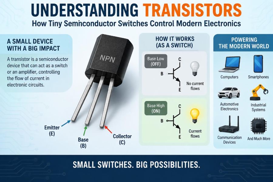

When a phone screen wakes, a laptop saves a file, or an electric car adjusts motor power, something extraordinarily small is making decisions at immense speed. Those decisions are not made by tiny mechanical levers. They are made by transistors: semiconductor devices that control the movement of electrical charge.
A single transistor may be almost invisible, yet billions can fit on one processor chip. They make digital logic possible, but they also shape radio signals, stabilize power supplies, amplify music, and drive LEDs.
For students, transistors connect circuit theory to real electronic systems. For working professionals, understanding their limits helps turn a schematic that appears correct into hardware that is efficient, reliable, and manufacturable.
The key idea is simple: a relatively small electrical input controls a larger current or voltage. The details behind that idea explain much of modern electronics.
🔍 What a Transistor Is
A transistor is a semiconductor device with three or more terminals. It can control current flow, act as a voltage-controlled or current-controlled source, and switch between operating states.
Unlike a passive resistor, capacitor, or inductor, a transistor can use energy from a supply to produce a controlled output. That controllability is why transistors are called active devices.
🧩 Why Three Terminals Matter
Three terminals allow one part of a circuit to influence another. In a bipolar junction transistor, or BJT, the terminals are the emitter, base, and collector. In a field-effect transistor, or FET, they are commonly called source, gate, and drain.
The control terminal is the base in a BJT and the gate in a FET. A signal applied there determines how readily charge carriers move through the main current path.
⚛️ Semiconductors Between Conductors and Insulators
Semiconductors conduct electricity neither as freely as metals nor as poorly as insulators. Silicon is useful because its conductivity can be deliberately changed by adding carefully selected impurities, applying electric fields, changing temperature, or exposing certain structures to light.
This adjustable behavior makes a transistor possible. The material can be engineered so that a small control signal changes the availability or movement of charge carriers.
🧪 Doping Creates N-Type and P-Type Material
Pure silicon has a crystal structure in which electrons are tightly shared between atoms. Doping introduces a very small amount of another element to alter the material’s electrical behavior.
N-type material has extra mobile electrons as its majority carriers. P-type material has an abundance of holes, which are useful ways of describing missing electrons that behave as positive charge carriers. Devices combine these regions in purposeful patterns.
🚦 The Junction That Controls Charge
Where p-type and n-type regions meet, a p-n junction forms. Charge redistributes near the boundary, creating a depletion region with relatively few mobile carriers.
Applied voltage can shrink or enlarge this barrier. A forward-biased junction more readily conducts; a reverse-biased junction strongly resists current until certain limits are exceeded. Transistor structures use this behavior more subtly than a simple diode does.
🧱 The Two Major Transistor Families
The most common introductory categories are BJTs and FETs. Both can amplify and switch, but their control mechanisms, input behavior, and preferred applications differ.
| Feature | BJT | FET, especially MOSFET |
|---|---|---|
| Control principle | Base current controls collector current | Gate voltage controls channel conductivity |
| Input current | Usually requires continuous base drive current | Very low steady-state gate current |
| Common strengths | Linear analog stages, predictable gain relationships | Digital ICs, efficient switching, power control |
| Key caution | Gain varies with device and conditions | Gate can be damaged by excessive voltage or static discharge |
The best choice depends on voltage, current, switching speed, linearity, thermal behavior, cost, and how the circuit will be driven.
🔺 How a BJT Controls Current
A BJT contains two p-n junctions arranged as either NPN or PNP. In a typical NPN transistor used as a low-side switch, a small current entering the base enables a much larger current to travel from collector to emitter.
In active operation, designers often use the approximation IC ≈ βIB, where β is current gain. It is an approximation, not a design guarantee: β can vary widely across devices, current levels, and temperature.
🌊 BJT Operating Regions
For basic circuit analysis, an NPN BJT is often described using cutoff, active, and saturation regions. In cutoff, base-emitter drive is insufficient and collector current is very small. In the active region, collector current is controlled by base drive and the device can amplify.
In saturation, both junctions are forward biased and the transistor is driven fully on for many switching uses. Saturation reduces voltage drop but can store charge, slowing turn-off in some circuits.
🚪 How a MOSFET Forms a Channel
A metal-oxide-semiconductor field-effect transistor, usually shortened to MOSFET, uses an insulated gate. In an enhancement-mode N-channel MOSFET, a sufficiently positive gate-to-source voltage creates a conductive channel between drain and source.
The gate’s insulating layer means essentially no DC gate current is needed after the gate voltage settles. However, the gate behaves like a capacitor, so it must be charged and discharged whenever the transistor switches.
📏 Threshold Voltage Is Not the “Fully On” Voltage
A common beginner mistake is treating the threshold voltage, VGS(th), as the voltage that turns a MOSFET fully on. Datasheets usually define threshold at a very small drain current under stated test conditions.
For low loss, the gate must often be driven well above threshold. Look instead for an on-resistance value, RDS(on), specified at the actual gate voltage you can provide. A 3.3 V microcontroller cannot automatically drive every “logic-looking” MOSFET efficiently.
🔀 Enhancement and Depletion Devices
Most modern switching circuits use enhancement-mode MOSFETs. They are normally off at zero gate-to-source voltage, making them convenient for controlled switching.
Depletion-mode devices are normally on and require an opposing control voltage to reduce conduction. They remain useful in specialized analog, protection, and current-source applications, but appear less often in beginner projects.
🔄 N-Channel and P-Channel Choices
N-channel MOSFETs generally offer lower on-resistance than comparable P-channel parts because electrons move more readily in silicon than holes. They are therefore common in low-side switches and many high-power arrangements.
P-channel MOSFETs simplify some high-side switches because pulling the gate below the source turns them on. The tradeoff is often higher resistance or a larger device for comparable performance.
💡 Transistors as Digital Switches
A digital circuit interprets voltages as logic states, but the transistor underneath is still an analog physical device. Designers aim to drive it into a state with either very little current flow or a low-resistance current path.
As an example, a microcontroller pin cannot safely power a motor directly. It can drive a transistor, while the transistor supplies the motor current from a separate power path. This is switching: a low-power signal controls a higher-power load.
📈 Transistors as Analog Amplifiers
In amplification, the transistor is intentionally biased between fully off and fully on. A small change at the input produces a larger controlled change at the output, drawing energy from the supply.
An audio preamplifier is a familiar example. The weak voltage from a microphone is not “made louder” by the transistor alone; rather, the transistor uses supply power to create an output signal with a larger usable amplitude.
🎯 Bias Sets the Useful Operating Point
Biasing is the DC setup that places a transistor at a desired operating point before the signal arrives. Without it, an amplifier may clip one half of the waveform, distort the signal, or become excessively sensitive to temperature and component variation.
Voltage-divider bias, emitter/source resistors, current mirrors, and feedback networks are common ways to make an operating point more stable. The exact method depends on topology and performance goals.
🧮 Load Lines Connect Device and Circuit
A transistor cannot choose any current and voltage independently; the surrounding supply and load impose constraints. A load line graphically shows the combinations allowed by the external circuit.
Where the load line intersects the transistor’s characteristic curves identifies the operating point. This graphical method is particularly useful for seeing why a collector resistor limits current and why a signal may eventually clip.
⚡ Voltage Drop and Power Dissipation
Whenever a transistor carries current while voltage exists across it, it dissipates power. For a switching MOSFET in the on state, conduction loss can be approximated as P ≈ I²RDS(on).
For a BJT used as a saturated switch, a practical estimate is P ≈ VCE(sat)IC. These simple expressions do not include every effect, but they reveal why a small voltage drop can still create substantial heat at high current.
🔥 Temperature Changes Device Behavior
Semiconductor parameters change with junction temperature. BJT base-emitter voltage, current gain, leakage, and MOSFET on-resistance all vary to some degree as a device warms.
Heat must travel from the silicon junction through the package and board into the environment. Datasheet thermal resistance values help estimate temperature rise, but actual layouts, copper area, airflow, mounting, and neighboring heat sources all matter.
🧯 Thermal Runaway and Current Sharing
Some operating conditions can create reinforcing feedback: more current causes more heat, and more heat encourages still more current. This is called thermal runaway. BJTs can be particularly vulnerable in parallel arrangements because warmer devices may take more current.
Emitter resistors, feedback, matched parts, careful thermal coupling, and active current control can improve sharing. MOSFETs often have more favorable current-sharing behavior at high currents because their on-resistance typically rises with temperature, but this is not a substitute for sound design.
⏱️ Switching Is Not Instantaneous
A transistor spends energy during transitions because voltage and current overlap while it moves between off and on. At low switching frequency this may be minor; at high frequency, switching loss can dominate conduction loss.
MOSFET gate charge, driver resistance, stray inductance, BJT storage time, and the load type all influence transition speed. Faster switching can reduce loss, but it can also worsen electromagnetic interference and voltage ringing.
🌀 Capacitive and Inductive Loads Need Different Care
Capacitive loads demand high current briefly while their voltage changes. Inductive loads, such as motors, relays, solenoids, and coils, resist changes in current and can generate high voltage when switched off.
A low-side transistor driving a relay usually needs a flyback diode across the coil. The diode provides a controlled path for stored magnetic energy after turn-off, protecting the transistor from a damaging voltage spike.
🛡️ The MOSFET Body Diode and Its Limits
Power MOSFET structures include an inherent body diode between drain and source. In some converter and motor-drive topologies, that diode conducts during part of a switching cycle.
Its existence does not mean every reverse-current situation is harmless. Forward voltage, reverse recovery behavior, current rating, and switching conditions must be considered. External diodes or carefully selected MOSFETs may be needed for efficient high-frequency designs.
📚 Reading a Transistor Datasheet
A datasheet is not merely a list of maximum ratings. It explains the conditions behind each number and often includes graphs that show how behavior changes with voltage, current, temperature, and drive.
- Maximum ratings: absolute limits, not preferred operating targets.
- On-state data:
RDS(on),VCE(sat), or gain under stated conditions. - Safe operating area: allowed voltage-current combinations for defined time intervals.
- Thermal data: junction limits and paths for heat removal.
- Dynamic data: gate charge, capacitances, switching times, and test circuits.
Always check the test conditions. A favorable headline value may apply only at a gate voltage, pulse duration, or temperature unlike your design.
🧭 Absolute Maximum Ratings Are Not Design Targets
A 60 V transistor should not automatically be used in a circuit expected to see 60 V. Supply tolerances, wiring inductance, load transients, startup events, and measurement uncertainty all consume margin.
Likewise, a package’s headline current rating may assume ideal cooling or a short pulse. Good selection includes derating: operating below limits to account for real conditions and long-term reliability.
🪜 Low-Side and High-Side Switching
A low-side switch sits between the load and ground. It is usually straightforward because an N-channel MOSFET’s source can remain near ground, allowing a logic-level gate drive.
A high-side switch sits between the positive supply and the load. It may be needed when the load must remain referenced to ground or when system architecture requires it. An N-channel high-side MOSFET often needs a gate voltage above the supply, requiring a dedicated driver, bootstrap circuit, or charge pump.
🎛️ Gate Resistors, Pull Resistors, and Drive Paths
A gate resistor can limit peak driver current, control switching speed, and reduce ringing. It is not automatically required at one fixed value; its choice depends on layout, driver capability, switching loss, and emissions.
A gate pull-down or pull-up resistor establishes a known off state while a controller resets or its pin is high impedance. Leaving a MOSFET gate floating can allow noise or stored charge to turn it partially on.
📐 Layout Is Part of the Circuit
At slow signals, a long wire may seem unimportant. During fast switching, every trace and wire has resistance, inductance, and capacitance. A high-current loop with excessive inductance can produce overshoot and ringing.
Keep switching loops short, use a low-impedance return path, place decoupling capacitors close to the power stage, and separate sensitive signal paths from noisy power paths where practical. A correct schematic can still fail because of poor physical layout.
📻 Transistors Enable Digital Logic
Complementary MOS, or CMOS, combines P-channel and N-channel MOSFETs to create logic gates. In a CMOS inverter, one transistor pulls the output high while the other pulls it low.
Ideally, one path is off in each steady logic state, so static power consumption can be low. Real chips still consume leakage power and switching power as internal capacitances charge and discharge, especially at high clock rates.
🧠 From Logic Gates to Processors
Logic gates made from transistors form adders, registers, memory cells, timing circuits, and control units. A processor is not one giant switch; it is an organized network whose transistor states represent and transform information.
Integration adds enormous capability, but it also hides the device level. Understanding the transistor remains valuable because timing, power, noise margins, and interface limits all trace back to physical electrical behavior.
📡 Radio, Sensors, and Power Electronics
Transistors are not confined to computers. In radio circuits they amplify or mix signals. In sensor interfaces they can buffer tiny currents. In voltage regulators and switching converters they control energy transfer through inductors and capacitors.
Different applications emphasize different transistor qualities. A low-noise amplifier values noise performance and linearity; a motor controller values voltage rating, current capability, thermal performance, and switching behavior.
⚠️ Common Beginner Mistakes
- Driving a transistor directly from a logic pin without calculating base current or gate-drive requirements.
- Assuming a MOSFET is fully enhanced at its threshold voltage.
- Omitting a flyback path for an inductive load.
- Using a breadboard for high-current or fast-switching power tests without recognizing its resistance and inductance.
- Trusting nominal transistor gain for a saturated BJT switch instead of providing adequate base-drive margin.
- Ignoring heat because the circuit works briefly on the bench.
These errors are common because a prototype may appear functional at light load. Testing at realistic voltage, current, temperature, and switching conditions is what exposes weaknesses.
🧰 A Practical Device-Selection Process
Start with the load: determine normal and peak current, supply voltage, inrush behavior, whether the load is inductive, and required switching frequency. Then choose voltage and current ratings with sensible margin.
- Choose the topology: low-side, high-side, half-bridge, linear stage, or another arrangement.
- Identify the available drive voltage and driver current.
- Estimate conduction and switching losses.
- Check thermal paths, package limits, and board copper requirements.
- Review protection for transients, reverse polarity, and fault conditions.
- Validate with measurements using probes and grounding methods appropriate for the switching speed.
This approach prevents selecting a transistor by one attractive datasheet number while missing the limitation that actually controls performance.
🧪 Building a Simple Transistor Switch Safely
A useful learning circuit is a low-side N-channel MOSFET switch driving a small DC load from a supply separate from a microcontroller’s logic rail. The grounds must share a reference, the gate needs a defined off-state resistor, and an inductive load needs a suitable flyback path.
Begin with a low-voltage, current-limited supply. Measure gate-to-source voltage, load current, and drain-to-source voltage while on. If the MOSFET has a larger voltage drop than expected, it may be inadequately driven, overloaded, or incorrectly connected.
🔬 Measuring What the Circuit Actually Does
A multimeter is excellent for DC checks, but an oscilloscope reveals switching edges, ringing, and transient behavior. Probe technique matters: a long ground lead can itself pick up noise and make a waveform look worse or different than the circuit node.
When diagnosing power switching, measure the relevant references. For a MOSFET, gate-to-source voltage is usually more meaningful than gate voltage measured only relative to an arbitrary system ground.
🌱 Scaling Down and Scaling Up
At the integrated-circuit scale, shrinking transistors enables dense digital systems but introduces leakage, variability, power-density, and fabrication challenges. At the power-electronics scale, larger devices handle substantial energy but demand careful packaging, cooling, isolation, and protection.
The governing principle remains the same across scales: electric fields and semiconductor structures regulate charge flow. What changes is the amount of power, speed, precision, and engineering margin required.
🧠 The Core Principle Behind Modern Electronics
Transistors matter because they let a circuit use a small signal to control a larger flow of energy or information. In switching, that produces clear on and off states. In amplification, it produces controlled analog variation. In integrated logic, it produces computation.
Reliable designs respect the real device rather than the ideal symbol: drive strength, voltage margin, heat, transition time, parasitic effects, and the load all shape the outcome. Once those constraints become familiar, transistor circuits stop looking like collections of mysterious symbols and start looking like deliberate systems of controlled charge.
A transistor is fundamentally a controllable path for charge, and mastering that path is the foundation for understanding nearly every modern electronic system. 🔌⚡🧠