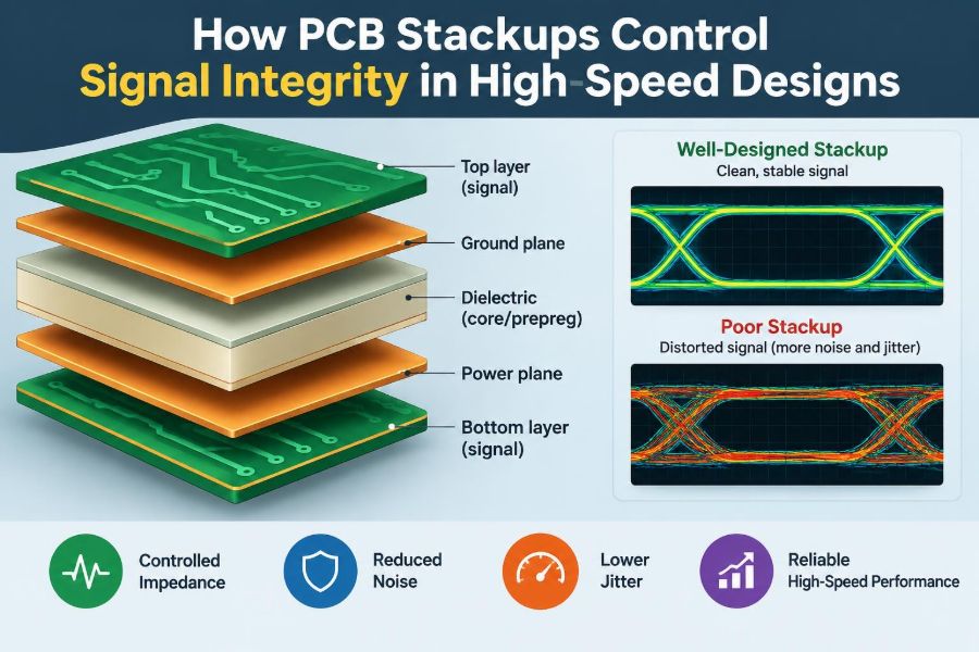

A prototype board powers up, the processor boots, and the low-speed interfaces appear normal. Then the memory link becomes intermittent, an Ethernet port drops packets, or a fast converter shows noise that was not present in simulation.
These failures are often blamed on a single trace, a connector, or a component placement detail. Yet the cause may have been decided much earlier: when the PCB layer stackup was chosen.
At high edge rates, a circuit board is not merely a place to connect parts. It is an electromagnetic structure that guides signals, provides return paths, stores energy, and couples unwanted noise between circuits.
A thoughtful stackup makes routing, power delivery, electromagnetic compatibility, and manufacturing work together. A weak stackup makes every later design decision harder. 🖨️
⚡ 1. Start with the real meaning of high speed
High speed is primarily about signal edge rate, not clock frequency alone. A digital clock at a modest repetition rate can still demand transmission-line treatment if its rising and falling edges are fast.
During a transition, the signal contains energy across a broad range of frequencies. If the trace is electrically long over that range, its impedance, delay, discontinuities, and return path all affect waveform quality.
This is why a stackup intended for slow control signals may fail when reused for a modern processor, serializer, RF interface, or high-resolution data converter.
🧱 2. See the PCB as an electromagnetic cross-section
A stackup specifies the order of copper and dielectric layers, their thicknesses, copper weights, material types, and sometimes impedance targets. It is the board’s vertical geometry.
That geometry determines the fields surrounding a routed trace. A trace on a layer near a reference plane behaves differently from one that is far from a plane or adjacent to a noisy routing layer.
Think beyond the visible top-layer artwork. For fast signals, much of the important behavior happens inside the dielectric between copper layers.
📐 3. Control impedance through geometry
Controlled impedance is the deliberate choice of trace width, copper thickness, dielectric height, and dielectric constant to create a target transmission-line impedance.
A single-ended trace may be designed as a microstrip or stripline. A differential pair is designed for both its individual trace behavior and the coupling between the two traces.
The fabricator needs an actual stackup, not only a nominal trace width. A width that produces the desired impedance on one buildup can be substantially different on another.
🌊 4. Understand why impedance discontinuities matter
When a propagating signal encounters a change in impedance, part of its energy reflects. Changes can arise at trace-width transitions, vias, connectors, component pads, layer changes, or plane voids.
A stackup cannot eliminate every discontinuity, but it establishes a stable baseline. Consistent dielectric spacing and well-defined reference planes prevent the entire route from behaving like a series of uncontrolled changes.
Reflections can cause ringing, overshoot, undershoot, timing uncertainty, and false threshold crossings. Their severity depends on driver behavior, termination, trace delay, and receiver characteristics.
🛤️ 5. Choose between microstrip and stripline
A microstrip is an outer-layer trace with a reference plane beneath it. Some of its electric field extends into air or solder mask, making it more exposed to its surroundings.
A stripline is routed between reference planes. Its fields are more contained, which usually improves isolation and reduces radiation, but it can have higher dielectric loss than a comparable outer-layer route.
| Structure | Useful characteristics | Common concerns |
|---|---|---|
| Microstrip | Accessible routing, easier probing, potentially lower dielectric loss | More radiation, environment-sensitive impedance, greater coupling to nearby features |
| Stripline | Strong field containment, stable reference environment, lower emissions | Harder probing, via transitions required, potentially more dielectric loss |
The best choice depends on interface speed, loss budget, routing density, test needs, and emissions requirements.
↩️ 6. Give every signal a continuous return path
Signal current leaves a driver through the signal conductor, but it must return to the source. At high frequency, return current concentrates near the signal’s reference conductor because the electromagnetic fields favor the lowest-inductance loop.
A nearby solid plane gives that current a predictable path directly under a single-ended trace. For a differential pair, the pair carries much of its own return current, but nearby planes still strongly influence common-mode behavior and field containment.
A fast trace without a continuous reference is not a controlled route.
🕳️ 7. Avoid splits and voids beneath fast routes
A plane split, antipad region, mounting hole clearance, or poorly placed copper cutout can interrupt the return path. The return current must then detour, increasing loop inductance and creating a discontinuity.
The result may include increased radiation, crosstalk, ground bounce, and degraded signal shape. A route that looks short in layout can have a much larger effective loop when its reference plane is interrupted.
Keep critical signals over uninterrupted reference copper. If a crossing is unavoidable, redesign the plane arrangement or provide a carefully engineered return-current transition close to the signal transition.
🔄 8. Manage reference changes at layer transitions
When a via moves a signal from a layer referenced to ground onto one referenced to power, or from one ground plane to another, the return current also needs a path between those references.
Ground-to-ground transitions can often use a nearby ground stitching via. A transition involving power and ground may need local decoupling that provides a high-frequency path between the planes.
Place the return transition close to the signal via. Separation enlarges the loop and turns a small routing event into an antenna-like structure.
📏 9. Dielectric thickness sets more than trace width
The distance between a signal layer and its reference plane strongly affects characteristic impedance. A thinner dielectric generally increases coupling to the plane and allows a narrower trace to reach a given impedance.
Close plane spacing also shrinks return-current loops, reduces radiation, and improves power-plane capacitance when the planes are a power-ground pair.
However, very thin dielectrics can create manufacturing constraints and may force trace widths or spaces that challenge the fabrication process. Stackup selection is an engineering trade-off, not a search for the thinnest possible layer.
🧪 10. Treat dielectric constant as a design input
The dielectric constant, often written as Dk, influences impedance and propagation delay. Materials do not necessarily have one perfectly fixed value under every frequency, resin-content, weave, and processing condition.
For a practical board, designers should use material data appropriate to the intended construction and ask the fabricator to model the finished geometry. Generic calculator defaults are useful for early estimates, not a final release.
Material variation matters more as timing margins and impedance tolerances become tighter.
🧶 11. Consider glass weave effects
Many laminates contain woven glass reinforcement. A trace routed over different parts of that weave can experience small local changes in effective dielectric behavior.
On long, tightly timed differential routes, unequal exposure can contribute to skew. Routing at an angle to the weave or selecting suitable material constructions can reduce the chance of persistent weave-related imbalance.
This is not a reason to panic over every digital net. It is a reason to match analysis depth to the interface margin and route length.
🔀 12. Build differential pairs into the stackup
Differential signaling relies on two conductors carrying complementary signals, but its performance depends on symmetry. Both traces should see similar geometry, dielectric environment, reference planes, and discontinuities.
Pair spacing changes differential impedance and coupling. Excessively tight coupling can complicate breakout and increase sensitivity to asymmetries, while excessively wide spacing weakens the pair relationship and can increase external field coupling.
Specify differential impedance with the stackup and route rules together. Do not select pair width and spacing independently of the layer geometry.
⏱️ 13. Control skew without creating unnecessary serpentine
In a differential pair, length mismatch produces delay mismatch. In parallel buses, mismatch can consume timing margin between related signals.
Length tuning should be applied after considering actual electrical delay, not simply visible route length. Different layers, via paths, and local dielectric environments can alter delay.
Large, tightly packed serpentine patterns may couple to themselves and distort the very delay correction they were meant to create. Use gradual tuning where possible and follow the interface’s real skew requirements.
📡 14. Reduce crosstalk by controlling fields
Crosstalk occurs when changing electric or magnetic fields from an aggressor route couple into a nearby victim. Parallel routing length, separation, layer arrangement, and reference-plane distance all matter.
A close reference plane helps confine fields near the intended trace and reduces coupling to adjacent routes. Routing signals on adjacent layers in perpendicular directions can also reduce broadside parallel coupling.
Useful routing habits
- Keep sensitive and aggressive nets separated on the same layer.
- Limit long parallel runs between unrelated high-speed signals.
- Use solid reference planes next to critical routing layers.
- Do not assume ground traces solve crosstalk unless they are well connected to a reference plane.
🧭 15. Assign layers according to signal purpose
A good stackup gives each layer a job. Outer layers may support components and short escapes, while inner layers provide controlled routing, solid references, or power distribution.
Critical signals benefit from layers directly adjacent to a continuous plane. Noisy switching nodes, slow control routes, and high-speed interfaces should not be treated as identical routing classes.
Layer assignment also makes reviews simpler because engineers can immediately see where sensitive routes are expected to live.
🔋 16. Use planes as part of the power-delivery network
Power and ground planes distribute DC current, but at high frequencies they are also part of the power-delivery network. Closely spaced power-ground planes provide distributed capacitance and a low-inductance path over part of the frequency range.
They do not replace local decoupling capacitors. Capacitors, planes, package connections, and voltage-regulator behavior form one network whose impedance changes with frequency.
A stackup that puts a power plane near ground can help contain power-plane fields and improve high-frequency current loops.
🧷 17. Place decoupling with the stackup in mind
A capacitor works best when its connection from power pin to power plane and ground plane has low inductance. Long traces, distant vias, and separated reference planes reduce its usefulness at fast transients.
Component-side power and ground access, via placement, and plane adjacency should therefore be planned together. The stackup can make a compact, low-inductance connection easy or awkward.
For dense devices, breakout strategy often determines whether decoupling connections are direct and short enough to support the intended power-delivery design.
🪜 18. Treat vias as transmission-line features
A via has inductance, capacitance, and a geometry that can differ greatly from the trace feeding it. At high data rates, via stubs can resonate and create impedance discontinuities.
Layer transitions should be minimized when they add no value. When transitions are necessary, use an appropriate pad, antipad, drill, and backdrill strategy based on the interface and fabrication capabilities.
Do not analyze a trace as controlled impedance and then ignore its via field. The channel includes both.
🧩 19. Coordinate breakout routing and BGA escape
Fine-pitch packages can force short traces through dense via fields before they reach an ideal routing layer. These escape regions are often among the most electrically constrained areas of the design.
Via-in-pad, microvias, buried vias, or alternative layer assignments may be considered, but each affects cost, yield, inspection, and supplier capability. The simplest manufacturable structure that meets electrical needs is usually preferable.
Discuss package escape early, before committing to an attractive but impractical layer count.
🏭 20. Design for the fabricator’s actual process
Stackups are manufactured constructions, not abstract drawings. Finished copper thickness, etched trace profile, resin flow, dielectric buildup, drill aspect ratio, and registration tolerance influence the final board.
Ask the fabricator for available materials and their controlled-impedance process. They can recommend practical widths and spaces for target impedance on a proposed construction.
Fabrication capability belongs in signal-integrity planning from the first stackup revision.
📋 21. Put clear impedance requirements in the fabrication data
Board documentation should identify which layers carry controlled-impedance traces, the target values, applicable trace types, and tolerance expectations agreed with the supplier.
It should also distinguish nominal design intent from dimensions the fabricator may adjust to meet impedance after accounting for their process. Ambiguity can lead to an electrically different board that is still manufacturable.
Useful documentation items
- Layer order and intended material system.
- Finished copper assumptions for signal layers.
- Target single-ended and differential impedances.
- Reference-plane assignments for critical layers.
- Whether impedance coupons or verification are required by the project.
🧮 22. Use field solvers instead of guessing
Closed-form impedance equations and online calculators are valuable learning tools, but real stackups include copper thickness, trapezoidal etch shape, solder mask, multiple dielectrics, and complex coupling.
A two-dimensional field solver models the cross-section more faithfully. It helps translate electrical targets into width and spacing rules before routing begins.
For especially demanding channels, broader simulation can include vias, connectors, packages, and termination networks. The model should be no more complex than needed to answer the design question.
📈 23. Simulate the complete channel
Signal integrity is a channel problem. Driver impedance, package parasitics, trace geometry, vias, connectors, receiver loading, and termination all contribute to the waveform at the receiver.
A beautiful stackup cannot rescue a poorly terminated channel, and an excellent termination cannot fully compensate for missing return paths or large via stubs. Analyze the interacting system.
For differential links, examine insertion loss, return loss, mode conversion, skew, and discontinuities where the available tools and interface requirements justify that level of study.
🔬 24. Verify assumptions on physical hardware
Simulation depends on models and assumptions. Prototype measurement reveals the combined effects of fabrication, assembly, packages, probes, fixtures, and operating conditions.
Oscilloscope probing must be done carefully; a long ground lead on a probe can add inductance and display ringing that is partly caused by the measurement setup. Differential probes, suitable fixtures, and calibrated network-analysis methods may be needed.
Test coupons can help validate impedance processes, while system-level measurements reveal whether the complete channel meets its functional margin.
🚫 25. Recognize common stackup mistakes
Many signal-integrity problems repeat because their root causes are easy to overlook during placement and routing.
- Routing fast signals on layers with no adjacent solid reference plane.
- Crossing plane gaps or changing reference planes without a return path.
- Specifying impedance without confirming the fabricator’s finished stackup.
- Putting two signal layers next to each other when a plane could isolate them.
- Using broad, uncontrolled outer-layer routes for sensitive interfaces.
- Adding length-tuning patterns without considering coupling and electrical delay.
- Leaving long via stubs in channels with limited loss or reflection margin.
Each mistake is easier and less expensive to prevent during stackup planning than to diagnose after boards arrive.
🗺️ 26. Apply the core stackup principle
The core principle is simple: every high-speed signal needs a predictable transmission path and a nearby, uninterrupted return path. Layer order, dielectric spacing, plane continuity, via strategy, and impedance rules all support that one goal.
Begin by classifying interfaces, power rails, packages, and mechanical constraints. Then create a candidate stackup, obtain fabricator feedback, derive routing rules, simulate the important channels, and verify the first hardware.
A PCB stackup is not a background manufacturing detail; it is an active part of the circuit that controls whether high-speed signals arrive cleanly and predictably. ⚡🧱📡