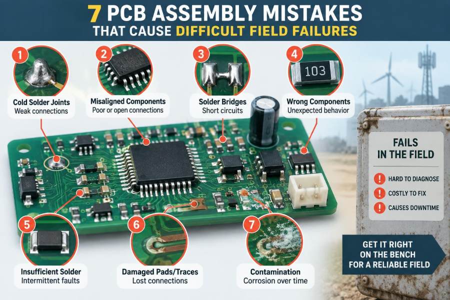

A controller works flawlessly during bench test, passes functional inspection, and ships on schedule. Months later, units begin returning from a humid factory floor, a vibrating vehicle, or a cabinet that cycles from cold nights to hot afternoons.
The fault reports are frustratingly vague: intermittent resets, missing sensor signals, random communication errors, or a board that starts working again after it is pressed, warmed, or allowed to dry. Nothing obvious appears in a quick visual inspection.
These are the failures that consume engineering time. They can involve an interaction between layout, materials, assembly process, handling, and the actual environment rather than one clearly defective component.
Most difficult field failures are not caused by a single spectacular mistake. They arise when a small process weakness leaves too little margin for real-world mechanical, thermal, electrical, or chemical stress.
🔍 1. Why PCB Assembly Details Matter in the Field
PCB assembly converts a design into a physical product. A schematic can be correct and the layout can satisfy design rules, yet unreliable joints, contamination, strain, or poor material control can still undermine the finished assembly.
Field conditions expose weaknesses that short production tests may not reproduce. Temperature change, vibration, moisture, power cycling, handling, and time all apply stress repeatedly.
🧭 2. The Seven Failure Families
The seven mistakes discussed here are common because each can hide behind apparently normal production results.
- Uncontrolled soldering profiles
- Inadequate land pattern and stencil design
- Moisture mishandling of sensitive parts and boards
- Residue and contamination left on assemblies
- Mechanical strain imposed on solder joints
- Weak inspection and test coverage
- Uncontrolled process changes and poor traceability
They are closely related. For example, a marginal solder joint may survive until board flexure or thermal cycling turns it into an intermittent open.
🔥 3. Mistake One: Treating Reflow as a Generic Heating Step
A reflow profile is not simply a recipe for making solder melt. It must transfer enough energy to form sound joints across a populated board without overheating components, laminate, flux, or solder paste.
Large inductors, shields, connectors, dense fine-pitch devices, and small passive parts do not heat at the same rate. A profile that looks acceptable at one measurement point may leave another area underheated or excessively hot.
🌡️ 4. What an Uncontrolled Reflow Profile Can Do
Insufficient time above liquidus or inadequate peak temperature can produce incomplete wetting, weak intermetallic formation, solder beads, or joints that look acceptable but have poor mechanical robustness.
Excessive heating can damage component packages, degrade laminate, cause warpage, accelerate oxidation, or exhaust flux before the joint forms properly. Both extremes reduce process margin.
- Fine-pitch packages may show opens, bridges, or head-in-pillow defects.
- Large thermal pads may have voiding or incomplete solder connection.
- Mixed-technology boards may expose through-hole joints to unnecessary thermal stress.
📈 5. Profile the Real Assembly, Not an Empty Coupon
Thermocouples should be attached to representative thermal locations on an actual populated board. Useful points often include a large ground pad, a small passive component, a dense integrated circuit area, and a thermally massive connector or shield.
Compare the measured profile with the solder paste supplier’s process guidance and the allowable limits of the most temperature-sensitive parts. Do not assume one profile fits every product family.
Revalidate when board stack-up, copper distribution, oven loading, panelization, component mix, or solder paste changes. Small changes can alter heating behavior significantly. 🌡️
🧩 6. Mistake Two: Using Footprints and Stencils Without Assembly Review
A CAD footprint that passes spacing checks is not automatically assembly-ready. Pad geometry, solder mask definition, stencil aperture, paste volume, component termination design, and placement accuracy must work together.
Assembly defects are often designed in long before production begins. The most reliable time to find them is during library review and design-for-manufacturing review.
📐 7. Land Patterns Control Solder-Joint Geometry
Pad dimensions influence how solder wets, where the component settles, and how much solder remains after reflow. Excessively small pads reduce termination overlap, while excessive pads can encourage component movement or undesirable fillet shapes.
Thermal pads under bottom-terminated components require particular care. If paste coverage is too high, trapped volatiles can increase voiding or float the package; if too low, thermal and electrical connection may suffer.
🧱 8. Stencil Apertures Are Process Components
The stencil determines deposited paste volume. It should not be treated as a direct copy of every copper pad, especially for fine-pitch parts, large exposed pads, and parts prone to tombstoning.
Aperture reduction, segmentation, rounded corners, and home-plate shapes can be useful responses to specific assembly risks. The correct choice depends on component geometry, board finish, paste, printing capability, and process evidence.
Examples worth reviewing
- Fine-pitch leads where excessive paste promotes bridging.
- Large QFN or power-device pads where segmented apertures can manage paste distribution.
- Small two-terminal passives where unequal heating or paste volume can lift one end.
- Connectors whose mechanical tabs need enough solder for strength.
⚖️ 9. Watch for Uneven Heating and Tombstoning
Tombstoning occurs when one end of a small chip component lifts during reflow. It is usually driven by an imbalance: one termination wets and pulls before the other side reaches similar conditions.
Unequal pad geometry, unequal copper heat sinking, inconsistent paste deposits, component orientation, and placement offset can all contribute. Simply increasing oven temperature does not solve the underlying imbalance.
Inspect the entire process chain: footprint symmetry, local copper, stencil apertures, placement, and thermal profile.
💧 10. Mistake Three: Ignoring Moisture Sensitivity
Many surface-mount packages absorb moisture from ambient air. During reflow, absorbed moisture can vaporize rapidly, creating internal stress in the package.
This may cause cracking, delamination, or separation that is not obvious externally. The device may pass initial electrical test and later fail after environmental or operational stress.
📦 11. Moisture Control Is a Time-and-Environment Discipline
Components classified as moisture sensitive are supplied with handling information that defines storage, floor-life, and baking requirements. That information should be part of the production traveler, not a document stored separately from the line.
Once dry packaging is opened, exposure time and ambient conditions matter. A practical system records when a reel or tray was opened, where it was stored, and whether its permitted exposure has been exceeded.
- Keep unopened dry-packed parts in appropriate storage conditions.
- Use dry cabinets or other controlled storage for opened material when required.
- Follow the component supplier’s instructions before baking material.
- Prevent accidental mixing of controlled and uncontrolled material.
🪵 12. Boards Can Hold Moisture Too
Printed circuit boards, especially after storage in humid conditions, can also contain moisture. Reflow can then cause laminate damage, surface anomalies, or delamination in susceptible constructions.
Board storage, packaging integrity, fabrication date, and any baking process should be controlled in the same disciplined way as component handling. Baking is not a universal cure; excessive or inappropriate baking can create other issues.
🧪 13. Mistake Four: Assuming “No-Clean” Means “No Risk”
No-clean fluxes are designed to leave residues that can often remain on a properly processed assembly. That does not mean every residue is harmless in every product, environment, or voltage domain.
Residue behavior depends on flux chemistry, activation level, reflow conditions, deposit amount, humidity, electrical bias, and contamination introduced elsewhere. A board that is benign in a dry office may behave differently in condensation-prone equipment.
🧂 14. Ionic Contamination Creates Hidden Leakage Paths
Salts, handling residues, poorly controlled cleaning chemistry, and some process residues can become electrically significant when moisture is present. Under bias, contamination can support leakage current and electrochemical migration.
The resulting symptom may be a high-impedance measurement error, false analog reading, communication instability, or a slowly developing short between conductors. These failures can disappear after drying, which makes diagnosis especially difficult.
🧤 15. Handling Practices Are Part of Electrical Reliability
Fingerprints, skin oils, fibers, adhesive residue, and uncontrolled rework materials can contaminate surfaces. Operators should use appropriate gloves or finger cots where required and avoid touching critical solderable or high-impedance regions.
Cleanliness requirements should be matched to product risk. High-voltage circuits, high-impedance analog inputs, fine-pitch assemblies, and harsh environments deserve more deliberate controls than a low-risk indoor product.
🧼 16. Cleaning Needs Validation, Not Hope
If a process includes cleaning, validate the complete process: chemistry, concentration, wash time, spray coverage, rinse quality, drying, board orientation, and compatibility with components and markings.
Partial cleaning can be worse than no cleaning when it redistributes residue into gaps beneath packages or leaves ionic wash residues behind. Define acceptance criteria and verify them with suitable inspection or cleanliness methods.
🪛 17. Mistake Five: Letting the Board Flex During Assembly
Modern assemblies often use small packages with solder joints that cannot tolerate much bending. Depanelization, connector insertion, screw fastening, test probing, heatsink attachment, and enclosure installation can all flex the board.
That flexure is transferred into solder joints and component terminations. The immediate result may be invisible cracking; the later result may be an intermittent failure when the product is handled or vibrated.
🧲 18. BGA and Ceramic Parts Need Special Mechanical Attention
Area-array packages can develop solder fatigue or pad-related damage when boards bend. Large ceramic capacitors are also vulnerable because ceramic bodies can crack under bending stress, producing leakage, capacitance changes, or eventual short circuits.
Keep high-strain operations away from vulnerable components where possible. Board support fixtures, component keep-out zones near breakaway tabs, and controlled depanelization methods reduce risk.
🔩 19. Connectors Need a Mechanical Load Path
A connector is not just an electrical component. Repeated mating, cable pull, vibration, and user handling apply force to the PCB.
Use mechanical tabs, stakes, chassis support, or other retention features where the application demands them. Do not rely on delicate signal pins alone to carry a recurring external load.
Also review connector placement near board edges and mounting holes. A mechanically sound solder joint can still fail if the local board region flexes excessively.
🛠️ 20. Rework Can Create a Local Reliability Defect
Rework is sometimes necessary, but it introduces another heating cycle and another opportunity for pad damage, contamination, misalignment, or thermal shock. A reworked board should not be assumed equivalent to an untouched board.
Use documented work instructions, appropriate tools, controlled materials, and inspection criteria. Record significant rework so recurring defects can be traced back to a process step or design feature.
👁️ 21. Mistake Six: Relying on Visual Inspection Alone
Visual inspection can detect obvious bridges, missing parts, polarity errors, solder balls, and poor wetting on visible joints. It cannot fully reveal hidden joints beneath BGAs, QFNs, shields, or connectors.
Nor can it prove electrical function, confirm every net connection, or predict whether a marginal joint will endure environmental stress. Inspection methods should be selected according to the failure modes that matter.
📷 22. Match Verification Method to Defect Mechanism
| Method | Especially useful for | Important limitation |
|---|---|---|
| Automated optical inspection | Presence, polarity, visible solder conditions, placement | Cannot see many hidden joints |
| X-ray inspection | Hidden solder joints, void patterns, bridges under packages | Interpretation and coverage need planning |
| In-circuit test | Net continuity and component-level electrical checks | Requires access and suitable test design |
| Functional test | System behavior under defined conditions | May miss latent mechanical or environmental defects |
No single method is sufficient for every board. The best test strategy combines complementary methods based on product risk and accessible evidence.
🧷 23. Design Test Access Before Layout Is Frozen
Test points, programming access, fixture clearances, boundary-scan capability, and controllable power domains should be considered during design. Retrofitting testability after layout release is costly and often incomplete.
A good test plan also defines what data to retain. Serial number, firmware version, test result, station, operator or automated station identity, and date can make later investigation far more efficient.
🔄 24. Mistake Seven: Allowing Silent Process Changes
Changing solder paste, board finish, stencil supplier, placement program, reflow oven, component source, cleaning chemistry, or panel design can change reliability. A change that improves yield in one area may introduce a new failure mode elsewhere.
The danger is not change itself. The danger is making change without assessing its effect, documenting it, and validating the outcome.
📝 25. Build a Practical Change-Control Loop
A useful change process identifies what changed, why it changed, which assemblies are affected, what risks are plausible, and what evidence is needed before broad release.
- Review substitutions for package, finish, moisture, and thermal differences.
- Assess whether assembly instructions, profiles, stencils, or test limits need updates.
- Run a controlled evaluation build when the risk justifies it.
- Record approval, lot boundaries, and resulting quality data.
This discipline makes it possible to distinguish a random field event from a failure associated with a specific material or process transition.
🏷️ 26. Traceability Turns Returns into Engineering Evidence
When a returned product has no traceable build history, investigators are forced to speculate. With meaningful records, they can compare affected units by production date, board lot, component lot, rework history, test record, and process revision.
Traceability does not have to mean collecting every possible datum. It means preserving the information needed to connect a physical unit to the decisions and materials that created it.
🌦️ 27. Reproduce the Real Stress, Not Just the Symptom
An intermittent unit should be examined under conditions that reflect its use. Controlled temperature change, humidity exposure, vibration, power cycling, connector movement, or gentle board flexing may reveal the sensitivity more effectively than repeated room-temperature functional tests.
Use safe, documented methods and avoid turning diagnostic stress into accidental damage. The goal is to identify a repeatable failure mechanism, not merely to make one sample stop working.
🔬 28. Investigate Failures Without Destroying the Clues
Start with non-destructive evidence: photographs, visual inspection, electrical measurements, X-ray where appropriate, and comparison with known-good units. Preserve the as-returned state whenever possible.
Only then move to more invasive analysis. Removing a component, cleaning a board, or reheating a joint may eliminate the very evidence needed to explain the failure.
A disciplined investigation sequence
- Document the reported symptom and operating context.
- Confirm the symptom with controlled measurements.
- Compare the unit with a known-good assembly.
- Review traceability and relevant process history.
- Form a mechanism-based hypothesis and test it.
- Correct the process, then verify the correction.
🧠 29. Prevention Is a Cross-Functional Task
Reliable assembly is shared work. Designers influence pad geometry, copper balance, component selection, board stiffness, and test access. Manufacturing engineers control materials, profiles, equipment, and work instructions.
Quality teams define evidence and response systems, while service teams provide the environmental details that turn a vague return into a useful reliability signal. The strongest organizations close the loop among all four groups.
✅ 30. The Core Principle: Protect Process Margin
The central lesson is simple: difficult field failures thrive where process margin is thin and evidence is missing. A joint, component, or surface that is only barely acceptable at the factory has little reserve for humidity, vibration, aging, or thermal cycling.
Control the thermal process, design pads and stencils for assembly, manage moisture, keep assemblies clean, prevent mechanical strain, inspect intelligently, and document change. These practices transform PCB assembly from a final production step into an engineered reliability process.
The most reliable electronics are built by treating every assembly detail as a potential field condition waiting to happen. 🛠️🔍🌦️