
Your phone charger has become small enough to slip into a pocket, yet it can deliver far more power than the bulky adapters of a decade ago. An electric vehicle can recharge faster, a solar inverter can waste less harvested energy, and a data center can pack more computing into the same floor area.
Those changes do not come only from smarter control software or better batteries. Much of the progress happens in the power converter: the hardware that changes electrical energy from one voltage, current, or waveform into another.
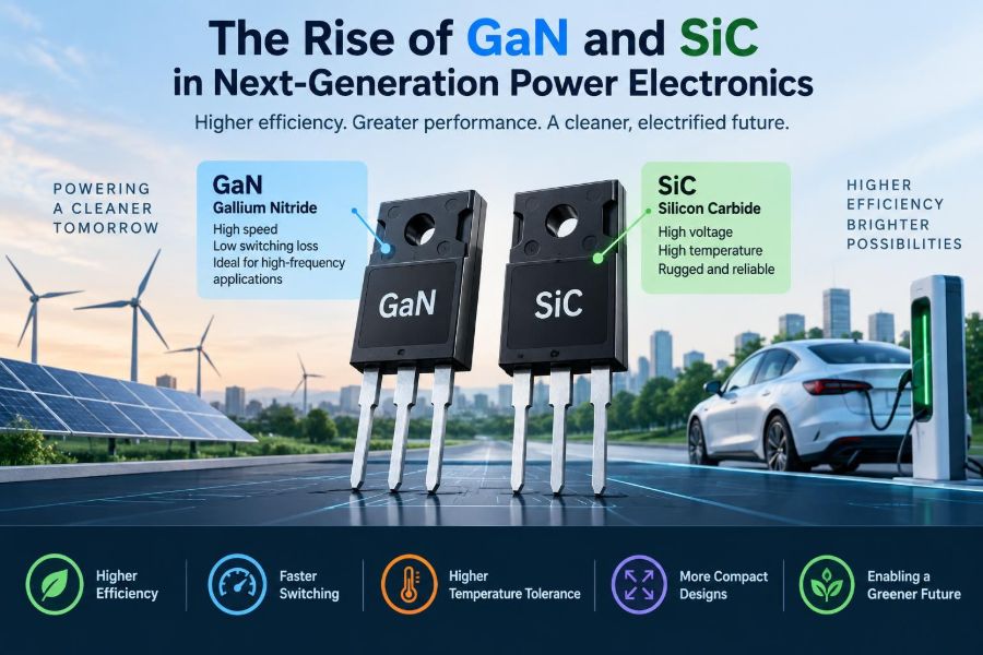
For decades, silicon was the default material for the transistors inside these converters. It remains indispensable. But as systems demand higher voltage, higher frequency, smaller size, and lower loss, two materials are moving from specialist applications into mainstream designs: gallium nitride (GaN) and silicon carbide (SiC).
Their rise is not a simple story of one semiconductor replacing another. Each solves a different set of engineering constraints, and using either successfully requires new thinking about circuits, layout, packaging, thermal design, and measurement.
🔌 Power electronics is the hidden energy interface
Power electronics controls the flow of electrical energy rather than merely processing information. A converter may turn AC mains into DC for a laptop, raise a battery voltage for a motor drive, or synthesize controlled AC for a solar grid connection.
At the center of many converters is a switching transistor. It repeatedly turns on and off, directing energy through inductors, transformers, capacitors, and loads. The ideal switch would change state instantly and lose no energy; real switches always dissipate some power.
🧱 Why conventional silicon approaches its limits
Silicon MOSFETs and insulated-gate bipolar transistors (IGBTs) are mature, capable devices. Their manufacturing ecosystem, models, packages, and design knowledge are enormous advantages.
However, higher voltage ratings generally bring higher resistance or slower switching in silicon MOSFETs. IGBTs handle high voltage and current effectively but have switching behavior that makes very high-frequency operation less attractive. These tradeoffs can make magnetics, heat sinks, and filters larger than designers want.
🧪 Wide-bandgap materials change the starting physics
GaN and SiC are called wide-bandgap semiconductors because their electronic bandgaps are wider than silicon’s. The bandgap is the energy needed to move an electron into a conducting state.
That property contributes to higher electric-field tolerance, lower leakage at elevated temperature, and the potential for fast switching. It does not eliminate losses, but it gives device designers a more favorable physical foundation for demanding power applications.
📊 The basic material comparison
| Characteristic | Silicon | GaN | SiC |
|---|---|---|---|
| Typical strength | Cost-effective, mature, broad range | Very fast, low-voltage-to-mid-voltage switching | High-voltage, high-power, high-temperature operation |
| Common device form | MOSFET or IGBT | HEMT power transistor | MOSFET or diode |
| Typical application focus | General power conversion | Compact adapters, telecom, RF-related power | EV traction, charging, industrial and grid systems |
| Design challenge | Loss versus size tradeoff | Fast-edge layout and gate control | Cost, packaging, and high-voltage insulation |
These categories overlap. Device ratings, package technology, control requirements, and supplier choices matter as much as material names. A material alone does not determine the best converter architecture.
⚙️ What makes GaN devices fast
Many power GaN devices are based on a high-electron-mobility transistor, or HEMT. Their structure creates a highly conductive channel, allowing low resistance and rapid switching in devices commonly used at a few hundred volts.
Low capacitances and the absence of certain reverse-recovery effects associated with silicon body diodes can reduce switching loss. This is especially useful when a converter must switch hundreds of thousands or even millions of times per second.
🏔️ Why SiC excels at high voltage
Silicon carbide can tolerate much stronger electric fields than silicon. A high-voltage SiC device can therefore use a thinner, more heavily doped drift region than an equivalent silicon device, reducing resistance for a given voltage class.
That advantage becomes particularly compelling as voltage rises into applications such as electric-vehicle traction inverters, fast chargers, industrial drives, and grid-connected equipment. SiC also maintains useful behavior at junction temperatures that would be challenging for many silicon devices.
🔥 Conduction loss is only one part of efficiency
When a transistor is on, it loses energy because current flows through a finite resistance or voltage drop. For a MOSFET, this is often discussed through RDS(on), the drain-to-source on-resistance.
At turn-on and turn-off, voltage and current overlap briefly. The resulting switching energy repeats every cycle, so increasing frequency can rapidly increase total loss. Designers must evaluate both mechanisms over the expected operating range, not just read one attractive number from a datasheet.
⏱️ Switching frequency reshapes the converter
Higher switching frequency allows smaller inductors and transformers because energy can be transferred in shorter intervals. It can also move filter requirements to higher frequencies, where smaller passive components may be practical.
But frequency is not free. Core losses, copper losses, gate-drive power, electromagnetic interference, and switching loss all rise in different ways. GaN often makes a high-frequency design feasible; it does not automatically make every design better at the highest possible frequency.
🪶 Smaller magnetics enable smaller products
A familiar 65 W USB-C charger illustrates the system-level effect. A designer can use fast switching to reduce transformer and inductor volume, then use efficient synchronous rectification to reduce heat. The result can be a compact supply rather than a heavy wall adapter.
The hypothetical lesson applies beyond chargers: a transistor choice influences the size of components around it. The practical target is not the smallest transistor, but the best balance of losses, magnetics, cooling, safety spacing, and manufacturing cost.
🌡️ High-temperature capability is not a license to run hot
SiC devices can operate at high junction temperatures, but the surrounding system has limits. Capacitor lifetime, solder reliability, connector ratings, magnetic insulation, enclosure materials, and nearby sensors may all set a lower usable temperature.
Thermal capability is best treated as design margin. A cooler device generally improves reliability and makes performance less sensitive to a hot ambient environment or a partially blocked airflow path.
🚗 Electric vehicles are a major SiC driver
An EV traction inverter converts battery DC into controlled AC for the motor. Lower converter loss can reduce heat rejection requirements and may improve usable vehicle efficiency, especially where switching losses matter.
SiC is also used in onboard chargers and high-power DC charging equipment. Higher switching frequency can reduce passive-component size, while high-voltage capability supports vehicle architectures designed around higher battery-bus voltages. Benefits vary with drive cycle, topology, and cooling system, so they should not be treated as a fixed range increase.
☀️ Solar and storage systems need efficient conversion
Photovoltaic inverters must extract DC energy from panels and deliver grid-compatible AC. Battery storage adds bidirectional conversion, often requiring equipment to charge and discharge efficiently over many operating points.
SiC can be attractive in higher-power inverters because it combines high voltage capability with fast switching. GaN may fit lower-power or high-frequency stages. In either case, efficiency affects both operating energy loss and the size of cooling hardware.
🖥️ Data centers value watts and volume
In a data center, power passes through several stages before reaching processors and memory. Loss at each stage becomes heat that must also be removed, creating an additional cooling burden.
GaN is increasingly relevant in compact, high-density power supplies and intermediate bus converters. Fast devices can support architectures with smaller magnetics, but the performance gain depends on careful layout and an efficiency curve that remains favorable across light and heavy loads.
🔋 Consumer charging showcases GaN clearly
Compact USB-C chargers made GaN visible to many consumers, but “GaN charger” is not itself a quality guarantee. The adapter still needs adequate isolation, safe temperature behavior, correct USB Power Delivery control, robust capacitors, and sound mechanical construction.
GaN helps designers reduce size and improve efficiency at useful power levels. Whether a particular charger is cool, reliable, and safe remains a complete product-design question.
🔄 Reverse conduction deserves careful attention
Power switches frequently conduct current in the reverse direction during converter operation. Silicon MOSFETs use an intrinsic body diode; its reverse-recovery charge can create loss and current spikes when commutation occurs.
GaN devices have different reverse-conduction behavior, while SiC MOSFETs are often valued partly because their associated diode behavior is much better suited to fast switching than conventional silicon alternatives. The exact behavior is device-specific, so designers should use manufacturer characterization rather than simplistic material rules.
📐 Parasitics become visible at fast edge rates
Every real circuit contains unintended inductance and capacitance. Package leads, PCB traces, vias, current loops, transformer winding capacitance, and probe wires all contribute parasitic elements.
When GaN or SiC switches rapidly, even a few nanohenries of loop inductance can produce noticeable voltage overshoot. This is governed by the relationship V = L × di/dt: fast current change through stray inductance creates voltage. A layout that was harmless in a slower silicon converter can become unstable or overstressed.
🧭 Layout is part of the circuit, not an afterthought
The highest-priority layout task is minimizing the commutation loop: the path through the switching devices and their local DC-link capacitor. Keep that loop compact, wide, and physically close.
- Place high-frequency ceramic capacitors directly across the relevant power loop.
- Use short, low-inductance gate-drive paths and a dedicated gate return.
- Separate noisy power currents from sensing and control grounds.
- Plan current loops before routing convenience signals.
For fast power stages, the PCB geometry is effectively an electrical component with tolerances and performance consequences.
🎛️ Gate driving is a controlled switching problem
A gate driver must charge and discharge transistor gate capacitances quickly enough to meet loss targets, yet not so aggressively that ringing, false turn-on, or excessive electromagnetic emissions occur. The gate resistor is often a tuning element, not a universal fix.
GaN gate voltage limits can be tighter than those of familiar silicon MOSFETs. SiC devices may need negative gate bias in some designs, depending on device type and operating conditions. Follow the manufacturer’s recommended drive range and consider protection against abnormal gate-source voltage.
🛡️ Protection must match faster fault behavior
Fast, efficient switches can also experience destructive current rise very quickly during a short circuit. A controller that reacts adequately in a slow system may not protect a wide-bandgap stage with the same margin.
Useful protection strategies can include desaturation or current sensing where appropriate, cycle-by-cycle current limiting, fast gate shutdown, bus overvoltage monitoring, temperature sensing, and carefully designed fault sequencing. Their suitability depends on topology and device safe-operating behavior.
📡 EMI is a system design constraint
Fast voltage transitions produce common-mode currents through unavoidable capacitances to chassis, cables, heat sinks, and earth. These currents can cause conducted and radiated electromagnetic interference, or EMI.
Slowing an edge may reduce emissions but increase switching loss. Better solutions often combine modest edge shaping with minimized loop area, well-placed common-mode filtering, shielding where justified, thoughtful transformer construction, and clean return paths. Passing an EMI test is rarely solved by adding one filter component at the end.
🔍 Measurement can mislead fast-switching designs
Long oscilloscope ground leads add inductance and can create ringing that is not truly present at the device terminals. Conversely, poor probe placement can hide damaging overshoot.
Use measurement methods appropriate to the bandwidth and voltage involved: short ground springs where suitable, differential probes with adequate rating, current probes with verified bandwidth, and probing points close to the switching loop. Treat every waveform as a measurement result that needs context, not immediate proof of circuit behavior.
📦 Packages and modules determine practical performance
A die with excellent electrical properties can underperform in a package with excessive inductance or poor thermal resistance. Surface-mount GaN packages can offer very short interconnects, while high-power SiC modules manage large current, high voltage, and heat removal.
Package selection affects creepage and clearance, assembly process, inspection, cooling interface, and serviceability. In high-voltage work, insulation coordination and mechanical construction are as essential as transistor parameters.
💰 Device cost is not system cost
Wide-bandgap switches can cost more than an equivalent silicon device. That comparison is incomplete if it ignores reduced heat sinking, smaller magnetics, less copper, a smaller enclosure, or lower operating energy loss.
Conversely, a premium device can be a poor system choice if it requires expensive layout changes, elaborate EMI mitigation, or specialized manufacturing without delivering a meaningful product benefit. Evaluate the bill of materials, manufacturing yield, qualification effort, and operating cost together.
🏭 Manufacturing quality and supply strategy matter
Wide-bandgap supply chains have grown rapidly, but designers should still qualify more than nominal voltage and current ratings. Parameter distribution, package availability, second-source options, lifecycle status, and application support affect production risk.
For long-lived industrial products, establish a component strategy early. A board optimized tightly around one package may be difficult to redesign if availability changes, especially when high-speed layout and thermal interfaces are involved.
⚖️ Choosing GaN, SiC, or silicon
A useful first question is not “which material is best?” but “what is limiting this design?” If high voltage and substantial power dominate, SiC is often a strong candidate. If compact high-frequency conversion at lower bus voltage dominates, GaN may be compelling. If cost, simplicity, and modest switching speed dominate, silicon may remain optimal.
- Choose based on voltage class, power level, switching frequency, and duty cycle.
- Compare total losses at real load and temperature conditions.
- Include magnetic size, cooling, EMI, isolation, and manufacturing constraints.
- Prototype early enough to validate layout and measurements.
Hybrid systems are common. A single product may use silicon in auxiliary rails, GaN in a high-frequency stage, and SiC in the highest-voltage power path.
🧰 A practical evaluation workflow
- Define input range, output requirements, transient behavior, ambient conditions, and safety constraints.
- Select a topology before selecting a transistor family; topology strongly shapes device stress.
- Estimate conduction, switching, magnetic, and gate-drive losses across operating points.
- Create a layout-aware prototype with probing locations and protection provisions included.
- Measure efficiency, thermal behavior, ringing, fault response, and EMI early.
- Revise the whole power stage rather than treating the switch as an isolated substitution.
This workflow reduces a common error: replacing a silicon device with GaN or SiC on an existing board and expecting the original layout, driver, and protection network to remain adequate.
🚧 Common mistakes in wide-bandgap projects
The most common mistakes are usually system mistakes rather than semiconductor mistakes. Engineers may optimize a datasheet figure of merit while overlooking thermal paths, gate-loop inductance, passive-component losses, or converter control behavior.
- Assuming a faster switch always permits a higher frequency.
- Using a generic gate driver without checking voltage limits and propagation behavior.
- Ignoring light-load efficiency and standby requirements.
- Adding snubbers without identifying the physical ringing loop first.
- Testing only at room temperature and nominal input voltage.
A disciplined design identifies the dominant loss and dominant risk first. That prevents expensive optimization of a secondary problem.
🧠 Control and power hardware must evolve together
Digital controllers can exploit fast power stages through adaptive dead time, synchronous rectification timing, advanced modulation, and fault logging. Yet control code cannot compensate for poor power-loop layout or inadequate sensing bandwidth.
Conversely, faster switching can challenge current measurement because noise couples into shunts, amplifiers, and isolated sensors. Control engineers and hardware engineers need shared timing assumptions, grounding strategy, and test plans.
🌍 Efficiency has broader engineering value
Reducing conversion loss lowers energy waste and heat. In portable equipment, that can extend usable battery time or permit a smaller enclosure. In stationary equipment, it can reduce cooling demand and improve power density.
The sustainability picture is broader than operational efficiency, however. Semiconductor manufacturing, material sourcing, product lifetime, repairability, and disposal all matter. Efficient hardware is valuable, but responsible engineering should consider the complete lifecycle.
🔮 What the next phase may look like
Expect continuing improvements in device structures, integrated drivers, low-inductance packaging, power modules, and design tools. Integration can shorten critical loops and simplify assembly, but it may also reduce flexibility in selecting individual components.
Wide-bandgap adoption will likely expand where its system advantages are clear, rather than replacing silicon everywhere. Silicon technology also continues to improve and remains exceptionally competitive in many voltage and cost ranges.
✅ The core takeaway: optimize the whole converter
GaN and SiC matter because they expand what power converters can achieve: faster switching, higher voltage capability, lower loss in suitable conditions, and smaller passive components. Their real value appears when those device-level strengths translate into a better complete product.
The best next-generation power design is not the one with the newest transistor material; it is the one that balances semiconductor physics, topology, layout, thermal behavior, EMI, protection, cost, and reliability for its actual job.
GaN and SiC give engineers powerful new options, but they reward careful system thinking. Learn their strengths, respect their fast-switching consequences, and choose them where the entire converter—not just the datasheet—benefits. ⚡🔧🌱