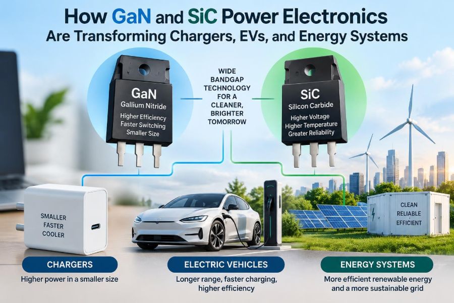

A laptop charger used to be a brick that warmed a desk and occupied half a travel bag. A phone charger was small, but charging larger devices quickly still meant carrying more weight, dealing with more heat, or accepting slower charging.
The same tension appears at a much larger scale in an electric vehicle, a solar inverter, or a factory motor drive. Engineers want to move more electrical energy with less loss, less cooling hardware, and less space—without compromising safety or reliability.
For decades, silicon has been the foundation of power electronics. It remains extraordinarily capable and cost-effective. But in applications where voltage, temperature, switching speed, or power density are pushed harder, two materials are changing the design options: gallium nitride (GaN) and silicon carbide (SiC).
They are not magic replacements for silicon. They are semiconductor materials with different physical strengths, and those strengths are reshaping chargers, electric drivetrains, renewable-energy converters, and the power infrastructure around them.
⚙️ Power Electronics: The Energy Traffic Controllers
Power electronics is the branch of electronics concerned with converting, controlling, and delivering electrical power. Its key devices act as extremely fast switches: they turn current on and off, steer it between paths, or reshape it into a useful voltage and frequency.
A USB-C charger converts high-voltage AC from the wall into regulated DC. An EV inverter converts battery DC into carefully timed AC for the traction motor. A solar inverter converts variable panel DC into grid-compatible AC. In all three cases, switching devices determine much of the size, heat, efficiency, and cost of the finished system.
🔄 Why Switching Creates Both Capability and Loss
An ideal power switch would have zero resistance when on, block all current when off, and change state instantly. Real transistors do none of these perfectly. They lose energy through conduction, switching transitions, gate-drive power, and associated components.
During a switching transition, voltage and current can briefly overlap. That overlap produces energy loss each cycle. At higher switching frequency, each individual event may be short, but it happens more often. Good power-semiconductor design is largely an exercise in managing these trade-offs.
🧱 Silicon’s Strengths—and Its Practical Limits
Silicon power MOSFETs, insulated-gate bipolar transistors (IGBTs), and diodes are mature technologies with extensive manufacturing capacity, design knowledge, and application support. For many low-cost or moderate-performance products, silicon remains the sensible engineering choice.
However, conventional silicon devices face increasing resistance and switching-loss challenges as voltage rating rises. High temperatures and very high switching frequencies can also narrow the practical design window. Designers may compensate with larger devices, lower frequency, additional cooling, or more complex converter arrangements.
🌐 What “Wide-Bandgap” Actually Means
GaN and SiC are called wide-bandgap semiconductors because the energy gap between their valence and conduction bands is wider than in silicon. This material property is linked to several useful high-power behaviors, including the ability to tolerate stronger electric fields and operate at higher junction temperatures.
The term does not mean that every GaN or SiC product will run hot or switch fast. Device structure, packaging, gate drive, layout, and operating conditions still matter. It means the underlying material gives designers room to pursue performance that is difficult to obtain with silicon alone.
⚡ GaN: Built for Fast, Compact Power Conversion
Gallium nitride power devices are especially attractive where fast switching and compact size matter. Most commercial power GaN devices are normally-off transistors designed for applications from low-voltage power conversion through several-hundred-volt power stages.
GaN devices can achieve very low capacitances and fast switching transitions. This can reduce switching losses and permit higher switching frequencies. Higher frequency is useful because inductors and transformers can often be made smaller when they handle energy in shorter, more frequent cycles.
🪨 SiC: Built for High Voltage and Harsh Conditions
Silicon carbide is particularly strong in high-voltage power conversion. SiC MOSFETs and SiC Schottky diodes are widely used in voltage classes relevant to EV traction inverters, fast chargers, industrial drives, rail systems, and solar or energy-storage converters.
SiC’s high electric-field capability allows a blocking-voltage device to use a thinner, lower-resistance drift region than a comparable silicon device. In practical terms, that can reduce conduction loss at elevated voltage ratings. SiC also retains useful characteristics at temperatures that would make silicon designs more difficult to manage.
🧪 The Material Differences Behind the Results
Two material traits are especially relevant. First, GaN and SiC can withstand stronger electric fields before breakdown. Second, SiC has high thermal conductivity, which helps move heat through the semiconductor material itself.
GaN is often associated with exceptional high-frequency behavior, while SiC is often selected for higher-voltage, high-power work. These are useful rules of thumb, not absolute boundaries. Product voltage rating, switching frequency, topology, thermal path, target cost, and supply availability should drive the final choice.
📊 GaN, SiC, and Silicon at a Glance
| Characteristic | Silicon | GaN | SiC |
|---|---|---|---|
| Typical strength | Mature, economical, broad use | Fast switching and compact converters | High voltage, high power, harsh thermal duty |
| Common power-device use | MOSFETs, IGBTs, diodes | High-frequency power transistors | MOSFETs and Schottky diodes |
| Often seen in | Mass-market power supplies and drives | Compact adapters and some data-center supplies | EV inverters, fast chargers, solar inverters |
| Design caution | Losses can rise in demanding conditions | Very fast edges challenge layout and EMI control | Cost, gate-drive details, and fast-edge effects |
This comparison describes broad application patterns, not fixed material laws. A well-designed silicon converter can outperform a poorly engineered wide-bandgap converter in its intended job.
🔌 Why Phone and Laptop Chargers Can Shrink
A compact charger needs an AC-to-DC conversion stage, isolation in many designs, filtering, control circuitry, and safe thermal performance. The magnetic components—especially the transformer and inductors—often occupy substantial volume.
When a GaN switch permits efficient operation at a higher switching frequency, the designer may reduce magnetic-component size while maintaining the same power output. Reduced loss can also reduce the need for large thermal spreaders. That is why some high-power USB-C adapters are notably smaller than older designs of similar output rating.
🌡️ Efficiency Is Mostly a Heat Story
Every watt lost inside a charger, inverter, or converter becomes heat that must be moved somewhere. In a tiny enclosed charger, a few watts of loss can make surface temperatures uncomfortable and force conservative power limits.
In an EV or industrial cabinet, loss affects cooling-system size, airflow, liquid-cooling demand, and component lifetime. A modest efficiency improvement can therefore create system-level benefits beyond electricity savings: smaller heat sinks, fewer fans, lighter enclosures, and more flexible packaging.
🚗 The EV Traction Inverter Opportunity
The traction inverter sits between an EV battery and motor. It switches battery energy into multiphase AC with timing that controls motor torque and speed. It handles substantial current and voltage, making its semiconductor losses highly consequential.
SiC MOSFETs can reduce switching and conduction losses in suitable high-voltage inverter designs. This can improve power density, ease thermal constraints, or support higher-voltage battery architectures. The practical outcome depends on the complete vehicle system; it should not be reduced to a universal claim about driving range.
🔋 Higher-Voltage EV Architectures
Raising the battery-system voltage for a given power reduces current. Since resistive cable loss scales with the square of current, lower current can reduce losses in conductors and make high-power charging more manageable.
Higher voltage also increases insulation, protection, connector, and component requirements. SiC devices are a natural fit in many of these systems because they are available for high blocking voltages with attractive loss characteristics. Yet high voltage alone does not guarantee a better vehicle; it changes several engineering trade-offs at once.
🏎️ Fast Charging Is a Whole-System Challenge
DC fast chargers must convert grid power into tightly controlled battery power while meeting isolation, protection, communication, and grid-quality requirements. Higher-power stations create demanding thermal and electrical conditions in both the charger and charging cable.
SiC can help reduce conversion losses and enable more compact high-power modules. But battery temperature, battery chemistry, state of charge, charger capability, cable cooling, and the vehicle’s charge-control strategy all influence charging time. The semiconductor is a key enabler, not the only limit.
☀️ Solar Inverters Need Efficient Voltage Conversion
Solar arrays produce DC power that varies with sunlight, temperature, and operating point. Inverters use maximum power point tracking and switching conversion to extract energy efficiently, regulate DC-link voltage, and deliver compliant AC power.
SiC devices can be useful where high DC voltage, high power, or compact installation is desired. Lower losses matter because inverter heat can limit output in hot environments. Higher switching frequency can also help reduce passive-component size, although filtering requirements and electromagnetic compatibility remain central design concerns.
🔋 Energy Storage Adds Bidirectional Power Flow
Battery energy-storage systems need converters that may charge batteries at one moment and discharge them the next. Some designs also support grid-forming or grid-support functions, demanding accurate and stable power control.
Wide-bandgap devices can improve the efficiency and density of bidirectional converters, particularly at demanding voltage and power levels. The benefit must be evaluated over real duty cycles. A storage system sitting idle most of the day may be influenced as much by standby consumption and control design as by peak switching efficiency.
🏢 Data Centers Value Power Density
Servers require multiple voltage-conversion stages, from building-level distribution to board-level processor rails. Heat is expensive because it must be removed reliably, often continuously.
GaN is appearing in high-frequency server power supplies and intermediate conversion stages where reduced conversion loss and smaller magnetics can increase power density. Less lost energy also reduces the cooling burden, though reliability, serviceability, and total system architecture remain just as important as transistor performance.
🏭 Industrial Drives and Motor Control
Variable-frequency drives regulate motor speed by producing controlled AC from a DC bus. They are used in pumps, compressors, conveyors, machine tools, and many other systems where motor energy use is significant.
SiC can offer benefits in high-performance drives, including reduced switching loss and potentially smaller filters or cooling hardware. However, very fast voltage edges can stress motor insulation and increase bearing-current concerns, especially with long motor cables. A faster switch requires a more deliberate system design, not merely a component substitution.
📡 Fast Edges Create EMI Work
A rapid voltage transition, often described by its high dv/dt, contains high-frequency energy. That energy can couple into cables, sensors, communication lines, and nearby equipment, producing electromagnetic interference (EMI).
GaN and SiC designs therefore demand careful layout. Engineers minimize high-current loop area, place decoupling capacitors close to switching devices, control return paths, and select appropriate filtering and shielding. In some cases, intentionally slowing an edge slightly produces a better overall system than pursuing the fastest possible transition.
🧭 Parasitics: The Hidden Circuit Elements
Every package lead, PCB trace, connector, and busbar has unwanted inductance and capacitance. At slow speeds these parasitics may be negligible. At wide-bandgap switching speeds, they can cause ringing, voltage overshoot, false gate triggering, and extra loss.
A useful analogy is a sharp tap on a long spring: energy bounces back and forth rather than stopping immediately. In a converter, the “spring” is distributed inductance and capacitance. Compact physical layout and low-inductance packaging are therefore core electrical requirements, not cosmetic refinements.
🎛️ Gate Drive Is Not a Generic Accessory
The gate driver commands a transistor to turn on and off, but its job extends beyond supplying a control voltage. It must manage timing, gate-loop inductance, protection behavior, isolation where needed, and resistance to noise.
GaN and SiC devices can have different gate-voltage limits and fault behavior from silicon devices. Designers must follow the device manufacturer’s guidance for gate resistance, negative bias where applicable, desaturation or overcurrent protection, and safe switching conditions. Copying a silicon gate-drive circuit without revalidation is a common and costly mistake.
🛡️ Protection Must Match Fast Faults
Short circuits, shoot-through events, overloads, and abnormal switching conditions can damage power devices extremely quickly. The protection circuit has to detect a problem and respond within the device’s actual capability.
Protection strategy may include current sensing, fast gate shutdown, active gate control, DC-link monitoring, temperature sensing, and coordinated controller firmware. The exact approach is topology- and device-specific. Designers should treat short-circuit withstand time as a critical design parameter rather than assuming all power transistors tolerate faults similarly.
🌡️ Higher Temperature Does Not Eliminate Thermal Design
Wide-bandgap devices may operate at higher junction temperatures than many silicon devices, but that does not mean higher temperature is automatically desirable. Heat still degrades materials, solder joints, capacitors, magnetic insulation, connectors, and nearby control electronics.
Thermal design begins with loss estimation and continues through package selection, interface materials, heat-spreader design, airflow or liquid cooling, and measurement under realistic load. The best result is often a cooler, more reliable assembly—not simply a semiconductor rated for a hotter junction.
📦 Packaging Can Limit the Device
A low-loss transistor inside a high-inductance package can lose much of its advantage. Package resistance, thermal resistance, creepage distance, isolation requirements, and module interconnects all shape final performance.
For high-power SiC systems, power modules and laminated bus structures can reduce parasitic inductance and improve thermal handling. For compact GaN converters, surface-mount integration and short PCB paths are valuable. The package and layout are part of the power switch’s effective behavior.
💰 Why Wide-Bandgap Devices Are Not Always Cheaper
GaN and SiC components can cost more than an equivalent silicon switch, and their surrounding design may require specialized drivers, packaging, testing, or EMI mitigation. Evaluating only transistor unit price can lead to the wrong conclusion.
A system-level comparison includes magnetics, cooling, enclosure volume, cable size, assembly, energy loss, and performance value. Conversely, if a product has generous space, modest switching frequency, and price-sensitive volume production, conventional silicon may remain the best overall solution.
🧩 Choosing Between GaN and SiC
There is no universal dividing line, but application tendencies are useful. GaN is often compelling in compact, high-frequency converters operating at lower-to-mid bus voltages. SiC is often compelling where voltage and power are higher, thermal conditions are demanding, or robust high-voltage switching is required.
- Consider GaN for compact adapters, telecom supplies, and high-frequency conversion where magnetics size is dominant.
- Consider SiC for EV traction, DC fast charging, high-voltage solar conversion, and demanding industrial power stages.
- Keep silicon in the comparison whenever its cost, maturity, and adequate performance make it the better system choice.
🧮 Topology Still Determines the Outcome
Device material does not replace converter architecture. A resonant converter, hard-switched bridge, multilevel inverter, active-clamp flyback, or interleaved stage each places different demands on switches, diodes, magnetics, and controls.
For example, a topology that achieves soft switching can reduce switching loss substantially, sometimes changing the value proposition of a device technology. Engineers should first understand voltage stress, current waveform, switching behavior, and fault requirements before choosing a semiconductor family.
🧰 A Practical Evaluation Workflow
Good selection starts with measurable requirements rather than material enthusiasm. Define the input and output range, power level, voltage class, duty cycle, cooling method, target volume, required lifetime, compliance needs, and acceptable cost.
- Estimate conduction, switching, magnetic, and auxiliary losses across the operating range.
- Model parasitic inductance, thermal paths, and worst-case voltage overshoot.
- Build hardware with measurement points for current, voltage, temperature, and conducted or radiated EMI.
- Test startup, shutdown, overload, short-circuit response, and abnormal line or load conditions.
- Compare complete system performance, not headline device specifications alone.
🔍 Measurements That Reveal Real Performance
Fast-switching measurements are easy to misread. Probe ground leads, bandwidth limits, poor probing locations, and measurement-loop inductance can create apparent ringing that is partly a test artifact.
Use suitable high-bandwidth differential voltage probes, low-inductance probing methods, correctly rated current sensors, and a carefully planned measurement reference. Correlate waveforms with thermal data and efficiency measurements. A clean-looking scope trace is not enough if the converter fails EMI, thermal, or transient testing.
⚠️ Common Design Mistakes
- Selecting a device based only on its lowest advertised on-resistance.
- Using a PCB layout intended for slower silicon switching without redesigning current loops.
- Ignoring reverse-conduction behavior, dead time, and commutation losses.
- Assuming higher allowable junction temperature solves an inadequate cooling path.
- Delaying EMI work until the mechanical enclosure and PCB are already fixed.
- Evaluating peak efficiency while ignoring light-load, standby, and thermal behavior.
These mistakes are connected: an overly fast edge may appear efficient at one operating point yet generate overshoot, EMI, and reliability stress that make the overall product worse.
🧱 Reliability Means More Than Surviving a Demo
Power hardware experiences thermal cycling, humidity, vibration, voltage transients, repetitive load changes, and occasional fault conditions. Reliability depends on die attach, bond or interconnect technology, package stress, capacitors, magnetics, connectors, cooling hardware, and controls.
Qualification must represent the application. A charger carried in a hot car faces different stress from a fixed solar inverter or a traction inverter exposed to vibration. Wide-bandgap devices enable new operating points, but every surrounding material must be validated at those conditions.
🌍 Grid Modernization Creates New Demand
Electrification adds power converters throughout the energy system: renewable generation, battery storage, EV charging, flexible loads, and high-efficiency industrial equipment. These converters must not only move energy efficiently; many must also respond intelligently to grid conditions.
GaN and SiC can make some conversion stages smaller and more efficient, helping equipment fit constrained spaces and reduce cooling demand. Still, grid resilience depends equally on controls, protection coordination, interconnection rules, communications, and the physical network.
🔮 What Adoption Is Likely to Look Like
Adoption will be uneven because applications have different pressure points. Consumer chargers may prioritize volume and compactness. Automotive designs must balance performance with supply continuity, qualification effort, and long service life. Utility-scale equipment emphasizes reliability, maintainability, and project economics.
Expect coexistence rather than a sudden replacement of silicon. Silicon will remain deeply embedded in power conversion, while GaN and SiC expand where their system-level benefits justify the added component and design complexity.
🎓 Skills Engineers Need for Wide-Bandgap Design
The most valuable skill is systems thinking. A power engineer needs semiconductor knowledge, but also magnetic design, PCB layout, electromagnetic compatibility, thermal analysis, control theory, safety isolation, and measurement discipline.
Students can build this capability by studying switching converters from schematic through layout and test. Working professionals can deepen it by reviewing real waveforms, failure analyses, and compliance results. Wide-bandgap projects reward engineers who connect physical implementation to circuit theory.
✅ The Core Takeaway: Better Materials Enable Better Systems
GaN and SiC are transforming power electronics because they can reduce losses and support faster or higher-voltage switching where silicon becomes constrained. Those properties can translate into smaller chargers, denser data-center supplies, more capable EV powertrains, and efficient converters for solar and storage.
The transformation is not caused by a material label alone. It comes from combining the right device with the right topology, package, layout, gate drive, protection strategy, thermal design, and validation plan. That is where the practical engineering value is created.
GaN and SiC matter most when their material advantages are designed into the complete power system, not simply swapped into an old circuit. For engineers, that makes wide-bandgap power electronics both a major opportunity and a reminder that details still govern performance. ⚡🔋🌍