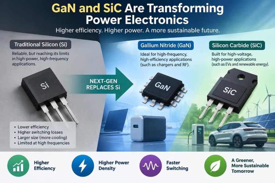

A phone charger that fits in a pocket, an electric vehicle that charges faster, and a solar inverter that wastes less of the day’s harvest may look like unrelated products. Behind all three is the same engineering challenge: switching and controlling large amounts of electrical energy with as little loss, heat, size, and cost as possible.
For decades, silicon has been the default material for power semiconductors. It remains extraordinarily capable, affordable, and deeply embedded in manufacturing. But as voltages rise, switching speeds increase, and space becomes scarce, conventional silicon devices encounter physical limits that circuit design alone cannot completely remove.
This is where gallium nitride (GaN) and silicon carbide (SiC) enter the picture. They are not universal replacements for silicon, nor are they simply “faster transistors.” They are wide-bandgap semiconductor technologies that change the trade-offs available to power-electronics designers.
Understanding those trade-offs matters whether you are selecting a MOSFET for a converter, designing an EV traction inverter, or trying to explain why a compact USB-C charger can deliver so much power without becoming dangerously hot.
⚙️ Power Electronics Is the Business of Energy Conversion
Power electronics uses semiconductor switches, magnetic components, capacitors, and control circuits to convert electrical energy from one form to another. A DC-DC converter changes one DC voltage to another; an inverter changes DC into AC; a rectifier does the reverse.
The central goal is not merely to move power. It is to control voltage, current, frequency, and direction efficiently. Every watt lost inside a switch becomes heat that must be conducted away, tolerated, or removed with cooling hardware.
🔌 Why Switching Devices Matter So Much
Modern converters usually operate by rapidly turning semiconductor devices on and off. During the on-state, the device ideally has zero voltage across it. During the off-state, it ideally carries zero current. In either ideal condition, power loss is zero.
Real switching is not instantaneous. Voltage and current overlap briefly during transitions, producing switching loss. In the on-state, a finite resistance or voltage drop creates conduction loss. Improving either loss mechanism can make an entire power system smaller and more efficient.
🧱 Silicon Built the Modern Power Industry
Silicon power devices include MOSFETs, insulated-gate bipolar transistors (IGBTs), diodes, and thyristors. Their manufacturing ecosystem is mature, their behavior is well understood, and their cost is often difficult for newer materials to match.
Silicon is therefore not disappearing. Low- and medium-voltage consumer products, industrial supplies, and many automotive systems will continue to use it extensively. The shift toward GaN and SiC happens first where silicon’s losses, voltage limits, or cooling burden become costly at the system level.
🧬 What “Wide Bandgap” Actually Means
A bandgap is the energy needed to move an electron from a bound state into a state where it can conduct through the material. GaN and SiC have wider bandgaps than silicon, hence the term wide-bandgap semiconductors.
This material property supports lower leakage at elevated temperature, stronger electric-field capability, and operation at higher temperatures than conventional silicon devices can generally tolerate. It does not mean every GaN or SiC component will automatically run hotter; package, gate-driver, capacitor, and reliability limits still matter.
📊 The Material Properties Behind the Change
Several physical properties shape power-device performance. A higher critical electric field allows a device to block a given voltage with a thinner, more heavily doped drift region. That can substantially reduce resistance in high-voltage devices.
GaN also offers high electron mobility in the active channel structure used by many power devices. SiC has excellent thermal conductivity, helping heat move through the semiconductor material. Each advantage affects a different part of the practical design problem.
| Characteristic | Silicon | GaN | SiC |
|---|---|---|---|
| Bandgap category | Conventional | Wide bandgap | Wide bandgap |
| Typical power strength | Cost-effective, broad voltage range | Very fast switching at lower-to-mid high voltages | High voltage, high temperature, high power |
| Common challenge | Losses rise at demanding voltage or frequency | Fast edges demand careful layout and protection | Device and system cost remain significant |
⚡ Higher Breakdown Fields Reduce Drift-Region Loss
A blocking power transistor needs a region that supports voltage when the device is off. In high-voltage silicon MOSFETs, this drift region becomes relatively resistive, increasing on-resistance.
Because SiC and GaN withstand stronger electric fields, their corresponding voltage-supporting regions can be more favorable electrically. This is one reason wide-bandgap devices become particularly attractive as voltage rises. The benefit is rooted in device physics, not just better packaging.
🔥 Heat Is a System Constraint, Not Just a Device Number
Losses determine heat generation, but thermal resistance determines how difficult it is to remove that heat. A lower-loss switch can allow a smaller heatsink, less airflow, a smaller enclosure, or more output power from the same physical volume.
SiC’s thermal conductivity is especially useful in high-power equipment. Still, a system’s weak thermal link may be solder, substrate, thermal interface material, or cooling plate rather than the semiconductor itself. Designers must analyze the complete thermal path.
⏱️ Why Faster Switching Changes Converter Size
Higher switching frequency can reduce the inductance and capacitance required for a converter. Smaller inductors and transformers can dramatically reduce volume and mass, which is valuable in adapters, aircraft systems, telecom equipment, and onboard vehicle chargers.
This is not a free gain. Magnetic core loss, AC winding loss, gate-drive loss, and electromagnetic interference generally increase with frequency. The useful question is not “what is the maximum switching frequency?” but “what frequency gives the best system-level compromise?”
🟦 GaN Devices: Built for Fast, Dense Conversion
Power GaN devices are commonly used as high-electron-mobility transistors, or HEMTs. Their structure forms a highly conductive channel through material interfaces rather than relying on the same geometry used by a conventional silicon MOSFET.
In many applications, GaN offers very low capacitance and fast switching behavior. This makes it compelling for compact AC-DC adapters, high-frequency DC-DC stages, data-center power supplies, and certain solar or battery conversion stages.
🎯 Where GaN Fits Best
GaN is often strongest where designers want high switching frequency and high power density at voltages commonly associated with offline power conversion and lower-voltage distribution. Compact chargers are a visible example, but the technology also serves more demanding equipment.
- USB-C and laptop power adapters
- High-frequency server and telecom power supplies
- Point-of-load and intermediate-bus converters
- Wireless-power systems and radio-frequency power applications
- Some motor drives and renewable-energy converter stages
The best fit depends on topology, voltage rating, power level, cooling, required isolation, and cost—not on the material name alone.
🧲 SiC Devices: Designed for High-Voltage Work
Silicon carbide is widely used in high-voltage MOSFETs and Schottky diodes. Its low resistance at high blocking voltages makes it particularly relevant in electric-vehicle traction inverters, fast chargers, industrial drives, rail systems, and grid-connected energy conversion.
SiC switching devices can reduce losses compared with silicon alternatives in suitable designs. That can increase usable range in an EV, reduce inverter cooling requirements, or permit higher switching frequency. The actual outcome depends on operating point and implementation.
🚗 Electric Vehicles Are a Major SiC Application
An EV traction inverter converts battery DC into controlled AC for the motor. It operates at high current, substantial voltage, and demanding thermal conditions. Even a modest efficiency improvement can matter because losses influence cooling demand and available battery energy.
SiC MOSFETs are attractive because they can combine high voltage capability with lower switching loss than many silicon solutions. They may allow designers to revisit motor-control frequency, passive-component size, and thermal architecture rather than simply swapping one transistor for another.
🔋 Higher Battery Voltage Changes the Equation
Higher-voltage vehicle battery architectures can reduce current for a given power level. Since cable and conduction losses scale with the square of current, this can reduce losses in conductors and enable powerful charging with more manageable currents.
However, higher voltage raises insulation, spacing, protection, measurement, and safety requirements. SiC’s high-voltage capability aligns well with this direction, but a vehicle platform requires coordinated design choices far beyond the inverter switch.
☀️ Renewable Energy Needs Efficient Conversion
Solar panels, batteries, and the AC grid operate at different voltage and current conditions. Inverters and DC-DC converters must manage those differences efficiently while meeting isolation, grid-quality, and protection requirements.
SiC can be valuable in larger solar and energy-storage inverters because voltage capability and efficiency are central concerns. GaN can be attractive in high-frequency auxiliary stages. The optimum choice varies with power scale, grid voltage, topology, and service expectations.
🏢 Data Centers Care About Every Conversion Stage
A data center may convert energy multiple times: from utility AC to facility distribution, then to rack-level distribution, then to voltages suitable for processors and memory. Losses at each stage accumulate into electricity use and cooling demand.
GaN’s fast switching can help reduce the size of high-frequency conversion stages. Yet the system benefit must include magnetics, capacitors, control behavior, redundancy, and serviceability. A highly efficient switch is useful only if the complete power architecture remains reliable.
🔄 Conduction Loss and Switching Loss Pull in Different Directions
Engineers often begin with two loss categories. Conduction loss is related to current and on-state resistance; in a simple resistive approximation, it rises with the square of current. Switching loss depends on voltage, current, switching frequency, and transition behavior.
A device with excellent low resistance is not automatically best at high frequency if its capacitances or reverse-recovery behavior are unfavorable. Conversely, a very fast device may not be the lowest-loss option in a low-frequency, high-current converter.
↩️ Reverse Recovery Is a Crucial Difference
Many silicon power circuits must account for reverse recovery: stored charge in a diode that must be removed when current direction changes. That charge can create loss, current spikes, and stress on the switching device.
SiC Schottky diodes have negligible reverse-recovery charge compared with conventional PN diodes. GaN devices also have different reverse-conduction behavior from silicon MOSFETs. Designers should study the specific device’s data-sheet behavior instead of assuming a familiar silicon body-diode model.
📈 Fast Edges Create New Problems
The same rapid voltage transitions that reduce switching loss can increase voltage overshoot, ringing, common-mode current, and radiated emissions. Parasitic inductance in a power loop turns a high rate of current change into unwanted voltage according to the familiar relationship V = L × di/dt.
With GaN especially, layout quality is not a finishing detail. It is part of the electrical design. A poor loop layout can erase efficiency gains, overstress devices, or create electromagnetic compatibility failures.
📐 PCB Layout Becomes a Performance Component
Keep the commutation loop—the path carrying rapidly changing switching current—small and compact. Place decoupling capacitors close to the switching devices, minimize vias in critical loops, and use a controlled return path for the gate-drive circuit.
High-current power routing and sensitive gate-drive or control traces should be thoughtfully separated. A layout that worked for a slower silicon MOSFET may behave badly after a fast GaN device is installed, even if the schematic appears unchanged.
🧠 Gate Driving Is Not an Afterthought
Gate-driver design determines how a power device turns on and off. It must provide appropriate voltage, current, timing, protection, and isolation where needed. An unsuitable driver can cause slow transitions, excessive ringing, false turn-on, or gate overstress.
GaN gate-voltage margins can be narrower than designers expect from robust silicon MOSFET practice. SiC MOSFETs also have specific drive-voltage and protection requirements. Use the manufacturer’s recommended operating limits and validate behavior with appropriate measurements.
🛡️ Protection Must Respond to Faster Faults
Short circuits, overloads, shoot-through, overvoltage, and abnormal switching conditions can destroy power devices quickly. Wide-bandgap switching speed may reduce the time available for detection and shutdown.
Effective protection can include current sensing, desaturation or overcurrent detection where applicable, active gate control, carefully designed clamps, undervoltage lockout, and fault-handling logic. The correct method is topology-dependent; protection should be tested under credible fault conditions, not assumed from simulation alone.
📦 Packaging Can Limit a Great Semiconductor
A low-loss die placed in a high-inductance package may not deliver its theoretical advantage at fast switching speeds. Package parasitics affect ringing, thermal resistance, current sharing, and the ability to use short switching transitions safely.
Modern power packages and module constructions aim to shorten current paths and improve heat extraction. When comparing devices, evaluate package, terminal arrangement, thermal data, and recommended layout along with headline resistance or voltage ratings.
🧪 Reliability Requires Application-Specific Thinking
Power semiconductors face electrical, thermal, mechanical, and environmental stress. Repeated temperature cycling can fatigue interconnects and solder layers. Humidity, contamination, vibration, voltage transients, and operating near maximum ratings can all affect field life.
GaN and SiC have growing application histories, but reliability evaluation should remain specific to the component, manufacturer, package, mission profile, and qualification evidence. A device proven in a charger may not automatically be suitable for a traction inverter or safety-critical industrial installation.
💰 Device Price Is Not the Same as System Cost
Wide-bandgap devices may cost more than a comparable silicon part. But a bill of materials should include heatsinks, fans, magnetics, enclosure volume, filters, cables, assembly complexity, and the value of energy saved over the product’s operating life.
A smaller magnetic component or eliminated cooling part can offset a higher transistor price. In other products, the cost premium may not be justified. Sound selection compares complete system economics rather than a single line item.
🧩 Not Every Silicon Design Needs a Replacement
Conventional silicon remains a rational choice where switching frequency is modest, voltage is well within silicon’s efficient range, thermal headroom is available, and low component cost matters most. Mature silicon solutions also offer broad sourcing and familiar design practices.
Replacing a switch without changing frequency, layout, gate drive, magnetics, and thermal design can produce little benefit. Wide-bandgap technology earns its place when the system requirements can use its capabilities.
🛠️ A Practical Device-Selection Workflow
Start with electrical requirements: maximum DC bus voltage, transient voltage, current waveform, switching frequency, ambient conditions, isolation needs, and target lifetime. Then estimate conduction and switching losses across the actual operating range, not only at one nominal point.
- Select a topology appropriate to the voltage, power, and isolation requirements.
- Compare silicon, GaN, and SiC candidates using realistic drive and temperature conditions.
- Model parasitics, then build a layout-conscious prototype.
- Measure switching waveforms with suitable high-bandwidth, properly referenced probes.
- Validate thermal performance, emissions, protection, and fault response before final optimization.
This process often reveals that the “best” device depends on a system constraint that was not obvious at the start.
🔍 Reading a Data Sheet Without Being Misled
Do not compare on-resistance values measured at different junction temperatures, gate voltages, or test currents as though they were identical. Likewise, capacitance values are voltage-dependent, and switching-energy figures depend on the stated test circuit and operating conditions.
Look for voltage derating guidance, gate limits, thermal impedance, safe-operating information, package inductance where available, body-diode or reverse-conduction behavior, and recommended layout. A data sheet is a starting point for engineering validation, not a guarantee of system performance.
📏 Measurement Techniques Need More Care at Fast Switching
Long probe ground leads can add inductance and display ringing that is partly created by the measurement setup itself. Differential probes, spring-ground techniques, current probes with appropriate bandwidth, and carefully chosen probe locations are often necessary.
Measure at the device terminals when practical, while respecting safety and instrument ratings. In high-voltage equipment, poor probing can be both misleading and hazardous. Follow established laboratory safety procedures and do not work on energized power hardware without suitable training.
🌐 Supply Chains and Manufacturing Still Matter
Material performance does not remove practical business risks. Availability, qualified second sources, package options, lead times, production test capability, and field-return analysis all influence whether a technology is suitable for a product line.
Demand for GaN and SiC has encouraged investment in manufacturing capacity and device development, but availability can vary by voltage class and supplier. Design teams should consider procurement resilience early, especially for long-life industrial and transportation products.
🧭 The Future Is a Mixed-Semiconductor Design Space
Power systems will not divide neatly into “old silicon” and “new wide bandgap.” Silicon, GaN, and SiC each occupy useful regions of voltage, current, frequency, cost, and reliability requirements. Hybrid architectures may use different technologies in different conversion stages.
Materials and packages will continue to improve, but the enduring engineering skill is matching device physics to system needs. The most successful designs treat semiconductor selection as one coordinated decision among topology, control, magnetics, mechanics, thermal design, safety, and manufacturing.
✅ The Core Takeaway for Power-Electronics Designers
GaN and SiC are replacing silicon in selected applications because they address limits that become expensive at high switching frequency, high voltage, high temperature, or high power density. GaN is especially compelling for very fast, compact conversion, while SiC is especially strong in high-voltage, high-power energy paths.
Neither technology is a universal upgrade. Their speed and efficiency introduce new requirements for layout, gate driving, protection, electromagnetic compatibility, measurement, and qualification. The breakthrough is therefore not only in the semiconductor material; it is in the ability to redesign the full power system around its strengths.
Choose GaN, SiC, or silicon by optimizing the complete converter—not by treating any one device technology as automatically superior. That approach turns promising material properties into reliable, useful engineering results. ⚡🔋🛠️