
Your phone charger is barely larger than a matchbox, yet it turns hazardous mains electricity into a carefully controlled low-voltage supply for sensitive electronics. A laptop adapter does the same job at far higher power, usually without becoming too hot to touch.
That compactness is not an accident. Older linear power supplies commonly relied on a large transformer operating at mains frequency, followed by circuitry that burned surplus voltage as heat. They remain useful in some applications, but they are often heavy and inefficient when substantial voltage conversion is required.
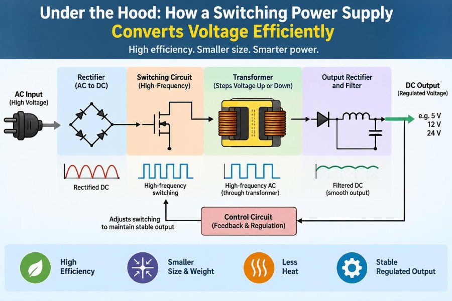
A switching power supply takes a different route. It turns energy flow on and off very rapidly, uses magnetic components at high frequency, and continuously adjusts those pulses to hold the output where it belongs.
The result is one of the most widely used ideas in practical electronics: efficient voltage conversion with important trade-offs involving noise, layout, safety, and control stability.
⚡ What a Switching Power Supply Actually Does
A switching power supply, often called an SMPS, converts electrical power from one voltage, current type, or isolation level to another by controlling semiconductor switches. The input may be DC from a battery, rectified AC mains, or another DC rail.
Its job is more than producing a nominal voltage. A useful supply must respond when the load changes, tolerate an expected input range, limit fault current, manage heat, and avoid injecting unacceptable electrical noise into the equipment it powers.
🔋 Why Voltage Conversion Is Necessary
Electronic systems need different voltages because their components have different electrical limits. A microcontroller may use 3.3 V, a motor may need 24 V, and a USB charging port may negotiate a higher voltage before conversion near the battery.
Converting voltage also lets designers distribute power more effectively. For a given power level, higher voltage means lower current, which reduces losses in cables and connectors. A converter near the load can then create the lower voltage needed by the circuit.
🔥 The Limitation of Linear Regulation
A linear regulator controls output voltage by behaving like a variable resistance. If it receives 12 V, delivers 5 V, and supplies 1 A, roughly 7 W is dissipated in the regulator under those conditions. That heat requires thermal design.
Linear supplies can be simple and exceptionally quiet, which is valuable for low-noise analog circuits. But when input and output voltage differ widely or load current is large, wasting the difference as heat is rarely practical.
✂️ The Central Idea: Rapid Switching
A power transistor is operated mainly in two states: fully on or fully off. When on, its voltage drop can be low; when off, ideally no current flows. In either ideal state, power dissipated in the switch is near zero.
Real switches have losses during transitions and due to resistance, capacitance, and leakage. Still, rapid switching can transfer energy far more efficiently than continuously dropping excess voltage across a linear element.
📦 Energy Storage Makes Conversion Possible
Switching alone does not create a stable new voltage. The converter needs elements that temporarily store and release energy: mainly inductors, transformers, and capacitors.
An inductor resists sudden changes in current by storing energy in a magnetic field. A capacitor resists sudden changes in voltage by storing energy in an electric field. Their behavior smooths a train of switching pulses into useful DC power.
🧲 Why High Frequency Shrinks Magnetics
A transformer or inductor operating at 50 or 60 Hz needs considerable magnetic material and copper to handle useful power without saturation. Raising the switching frequency allows a much smaller magnetic component for a similar energy-transfer role.
This is why compact chargers are feasible. Higher frequency is not free, however: switching losses, magnetic core losses, electromagnetic interference, and layout sensitivity generally become more challenging as frequency rises.
🔁 The Basic Switching Cycle
Consider a simple buck converter. During one part of the cycle, a switch connects the input to an inductor, causing its current to rise and storing energy. During the next part, the switch turns off and the inductor keeps current flowing into the load through an alternate path.
The output capacitor fills in the short-term difference between inductor current and load current. Repeating this cycle many thousands or millions of times per second produces a nearly steady output voltage.
⏱️ Duty Cycle Controls Average Voltage
The duty cycle is the fraction of each switching period for which a controlled switch is on. In an ideal buck converter operating in continuous conduction, output voltage is approximately input voltage multiplied by duty cycle.
If the input changes or the load suddenly demands more current, the appropriate duty cycle changes too. A controller measures the result and adjusts pulse timing, rather than relying on a fixed on-time.
⬇️ The Buck Converter Steps Voltage Down
A buck converter reduces DC voltage. It is common wherever a battery, adapter, or intermediate bus voltage must supply lower-voltage digital electronics.
For example, a board receiving 12 V may use buck converters to create 5 V, 3.3 V, and a tightly controlled processor rail. Its main advantage is that it transfers most energy rather than dissipating the voltage difference as heat.
⬆️ The Boost Converter Steps Voltage Up
A boost converter raises DC voltage. It first stores energy in an inductor while the switch is on. When the switch turns off, the inductor’s voltage reverses as it tries to maintain current, adding to the input and driving energy into a higher-voltage output.
This topology appears in devices that must make a higher rail from a single-cell battery, such as LED drivers or equipment needing a stable bus as battery voltage falls during discharge.
🔄 Buck-Boost Topologies Handle Both Directions
A buck converter cannot regulate when its input falls below the required output, while a conventional boost converter cannot reduce a high input. Buck-boost designs address cases where input can move above and below the target voltage.
Battery-powered products often need this flexibility. A lithium-ion cell, for instance, changes voltage significantly across its usable charge range, while downstream electronics may require a regulated rail that remains constant.
🧱 Flyback Converters Provide Isolation Simply
A flyback converter stores energy in a coupled magnetic component while its primary switch is on, then transfers that stored energy to the secondary side when the switch turns off. Although commonly called a transformer, its operation resembles a coupled inductor.
Flyback designs are widely used in lower-power isolated adapters because they can create one or multiple outputs with relatively modest component count. Their stresses, ripple current, and transformer design demand care.
🔌 Forward, LLC, and Other Isolated Families
At higher power levels, designers often select topologies that transfer energy while the primary switch is conducting, or that use resonant energy transfer. Forward-derived converters, bridge topologies, and LLC resonant converters are examples.
There is no universally best circuit. The choice depends on power range, input range, isolation requirement, allowable size, efficiency target, output regulation needs, cost, and expected electromagnetic emissions.
🛡️ What Electrical Isolation Changes
An isolated power supply uses a transformer so that input and output have no direct conductive connection. Isolation can protect users, break ground paths, and permit safe low-voltage outputs from mains-derived inputs when designed to applicable safety requirements.
Isolation is not simply a transformer added to a schematic. It requires correct insulation systems, physical spacing, safety-rated components, and a layout that preserves creepage and clearance distances. Mains supply design should be undertaken only with appropriate training, standards knowledge, and test capability.
🎛️ The Controller Is the Supply’s Decision-Maker
A controller IC generates gate-drive signals and determines when switches turn on and off. Some controllers use fixed-frequency pulse-width modulation, while others may vary frequency, use pulse skipping at light load, or apply resonant control methods.
Modern controllers often include soft start, current sensing, undervoltage lockout, synchronization, and fault protection. Integration simplifies designs, but the surrounding power stage still determines whether the supply behaves reliably.
📏 Feedback Keeps the Output Regulated
Without feedback, output voltage would drift with input voltage, load current, temperature, and component tolerances. A feedback network senses the output, compares it to a reference, and tells the controller whether to increase or decrease energy delivery.
In isolated supplies, feedback must cross the isolation boundary without defeating it. This may be done with an optocoupler or with techniques that infer output conditions from auxiliary windings, depending on required accuracy and topology.
📈 Compensation Prevents Unstable Regulation
The feedback loop needs compensation: deliberately chosen frequency response that keeps correction stable. If the loop reacts too aggressively or with too much phase delay, the supply can oscillate, ring after load changes, or produce excessive output ripple.
Compensation is one reason a converter cannot be treated as a collection of interchangeable parts. Inductor value, capacitor characteristics, switching mode, load range, and sensing method all influence the control loop.
🌊 Inductors and Capacitors Shape Ripple
Switching converters naturally create ripple because energy moves in packets. The output capacitor supplies or absorbs ripple current, while the inductor limits how quickly current changes. Their values and parasitic properties affect ripple amplitude and transient response.
A capacitor’s equivalent series resistance and inductance matter as much as its labeled capacitance at high frequency. Ceramic capacitors can have low resistance but their effective capacitance may vary with DC bias; electrolytic types offer bulk energy storage but may have higher resistance and shorter life under heat.
🧮 Continuous and Discontinuous Conduction
In continuous conduction mode, inductor current never falls to zero during normal operation. In discontinuous conduction mode, it reaches zero for part of each switching cycle, often at lighter loads or by deliberate design.
These modes alter current stress, ripple, control behavior, and the equations used for design. A converter may move between modes as load changes, so a stable design must account for its full expected operating range.
⚙️ Synchronous Rectification Reduces Loss
Many converters use a diode as the alternate current path or output rectifier. A diode’s forward voltage produces a loss proportional to current, which can become significant on low-voltage, high-current rails.
Synchronous rectification replaces that diode with a controlled MOSFET. When timed correctly, the MOSFET’s low on-resistance can reduce conduction loss. Incorrect timing can cause reverse current or shoot-through, so gate control is critical.
🌡️ Where Efficiency Is Lost in Reality
Efficiency is limited by more than the main transistor. Losses occur in MOSFET on-resistance, switching transitions, gate drive, diode drops, inductor winding resistance, magnetic cores, capacitor resistance, control circuitry, and PCB copper.
Light-load efficiency can differ sharply from full-load efficiency because fixed losses become a larger share of output power. A supply that performs well at one operating point may not be the best choice for an always-on device that spends most of its time nearly idle.
🌡️ Thermal Design Determines Lifetime
Every watt lost becomes heat somewhere. Junction temperatures affect semiconductor reliability, capacitor aging, and available output current. Thermal design therefore includes component selection, copper area, heat sinks where appropriate, airflow, enclosure properties, and realistic ambient temperature.
Do not assume a converter’s headline efficiency makes temperature irrelevant. Concentrated loss in a small package can still create a hot component, especially in sealed products or near other heat sources.
📻 Switching Noise Has Two Main Paths
Fast voltage and current transitions generate electromagnetic interference, or EMI. Conducted noise travels through input and output wires; radiated noise couples through electric and magnetic fields into nearby circuits, cables, or antennas.
Noise is not merely a compliance problem. It can disturb radio receivers, corrupt sensor readings, create audible artifacts, or cause unexpected behavior in high-impedance analog circuitry.
🗺️ PCB Layout Is Part of the Circuit
At switching speeds, trace inductance and loop area strongly influence voltage spikes and emissions. The highest-current switching loop should be physically small, with short, wide connections and carefully placed input bypass capacitors.
Keep the noisy switch node compact and away from feedback traces. Route sensitive sensing connections deliberately, provide a controlled return path, and follow the controller manufacturer’s layout guidance as a starting point rather than an afterthought.
🧯 Snubbers and Clamps Tame Voltage Spikes
Parasitic inductance stores energy too. When current through it is interrupted quickly, it can create a voltage spike that stresses switches and radiates noise. This is especially visible around transformer leakage inductance in isolated converters.
RC or RCD snubbers, TVS devices, active clamps, and carefully designed resonant transitions can manage these spikes. Each approach trades complexity, loss, voltage stress, and control requirements differently.
🚧 Protection Features Handle Abnormal Conditions
A well-designed power supply expects faults. Common protections include cycle-by-cycle current limiting, short-circuit response, output overvoltage protection, input undervoltage lockout, overtemperature shutdown, and soft start to control inrush current.
Protection thresholds and recovery behavior matter. A supply that repeatedly starts and shuts down into a fault may be appropriate in one product, while another application needs a latched shutdown or controlled current limit to avoid damage.
🔍 Reading a Converter Datasheet Wisely
A regulator IC datasheet provides conditions, not promises that any surrounding circuit will work. Check the permitted input range, switching frequency, current-limit method, recommended inductor range, compensation guidance, thermal information, and test conditions behind electrical specifications.
Also inspect application circuits critically. A reference layout may be optimized for a particular board, load range, or capacitor family. Copying values without understanding their function is a common path to marginal performance.
🧪 Measuring a Supply Without Misleading Yourself
Measure input and output power with instruments suited to the waveform and voltage involved; efficiency is output power divided by input power under defined conditions. A multimeter alone may not reveal ripple, short spikes, startup behavior, or control-loop instability.
For oscilloscope ripple measurements, use a short ground spring or equivalent low-inductance probing method. A long probe ground lead can act like an antenna and display ringing that belongs mainly to the measurement setup.
🛠️ A Practical Design Workflow
Start with requirements before selecting a topology. Define input range, output voltage tolerance, maximum and minimum load, isolation need, acceptable ripple, ambient temperature, size constraints, expected operating modes, and safety or EMC obligations.
- Select a topology appropriate to voltage relationship, power level, and isolation requirement.
- Choose a controller and calculate initial power components using validated design guidance.
- Lay out the critical current loops before treating the board as complete.
- Test startup, load steps, input extremes, thermal behavior, faults, and emissions early.
- Revise component values and layout based on measurements, not assumptions.
🚫 Common Mistakes That Reduce Performance
- Choosing an inductor only by inductance: saturation current, RMS current rating, resistance, core loss, and temperature rise also matter.
- Ignoring capacitor derating: actual capacitance and ripple-current capability can differ from a nominal label in operation.
- Using long switching loops: this increases ringing, switch stress, and EMI.
- Testing only at one load: startup and light-load modes often expose different problems.
- Treating thermal and safety review as late tasks: these constraints can require major layout or topology changes.
🎯 Choosing Between Switching and Linear Supplies
A switching regulator is usually the preferred choice when power is substantial, voltage difference is large, battery runtime matters, or compact size is needed. It can deliver excellent results, but demands more design attention than a basic linear regulator.
A linear stage may still be sensible after a switcher when a small amount of voltage must be dropped and very low noise is required. The best architecture sometimes uses both: efficient switching conversion first, then local linear cleanup for a sensitive circuit.
🧠 The Core Principle to Remember
Switching power conversion is controlled energy transfer. The switch chops energy into manageable intervals, magnetic components store or transfer it, capacitors smooth it, and feedback decides how much arrives on the next cycle.
Efficiency comes from keeping components close to their low-loss operating states, not from eliminating loss altogether. Successful designs balance that efficiency against ripple, noise, cost, thermal limits, transient behavior, manufacturability, and safety.
A switching power supply converts voltage efficiently by moving energy in precisely controlled packets rather than burning unwanted voltage away as heat. Once that picture is clear, topology choices, feedback loops, magnetics, layout, and protection features all become connected parts of the same engineering problem. 🔌⚙️📈