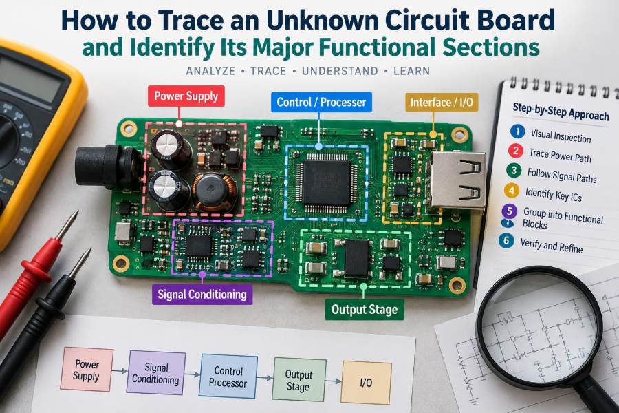

You find a circuit board in a discarded instrument, an industrial controller, or a piece of equipment with no schematic. It may look like a dense field of copper tracks, anonymous black packages, and connectors that reveal very little at first glance.
The temptation is to begin probing every pin. A better approach is to treat the board as a physical record of engineering decisions. Power has to enter somewhere, signals have to travel somewhere, and components are placed to support those jobs.
Tracing an unknown printed circuit board (PCB) is a practical skill for repair, reverse engineering, fault finding, and learning. It is not about guessing what every part does immediately; it is about building a reliable map, one observation at a time.
With a multimeter, careful photographs, and a disciplined sequence, even a complicated board becomes a set of recognizable functional sections rather than an intimidating collection of parts.
🧭 Start with a Functional Mindset
A circuit board is usually easier to understand as a system than as a list of components. Most electronic products contain some combination of power input, regulation, processing, sensing, communication, output driving, and protection.
Your first goal is to identify these broad blocks and the connections between them. A microcontroller may remain unidentified, for example, yet you can still determine that it receives regulated power, reads several inputs, and drives a display or actuator.
This top-down view prevents a common mistake: spending an hour identifying a single resistor network before knowing whether it belongs to the power supply, an input circuit, or a communication interface.
⚠️ Decide Whether the Board Is Safe to Handle
Before tracing anything, consider what equipment the board came from. Mains-powered appliances, battery packs, motor drives, inverters, televisions, and power supplies can contain hazardous voltages or retain charge after disconnection.
Look for large electrolytic capacitors, wide isolation gaps, warning symbols, mains-rated connectors, fuses, transformers, and optocouplers. These features often indicate a high-voltage section, which should be treated differently from low-voltage logic.
- Disconnect all power sources and removable batteries.
- Do not assume a capacitor is discharged because an indicator LED is off.
- Use suitable discharge procedures and test equipment if high energy is possible.
- Do not connect a USB oscilloscope or grounded bench instrument across a live mains-referenced circuit without understanding the grounding consequences.
Tracing a board while unpowered is the safest and most informative first stage. Power should only be applied later, with a reason and an appropriate current-limited setup.
📷 Record the Board Before Touching It
Take clear, high-resolution photographs of both sides before removing parts, cleaning flux, or adding probe marks. Include connector faces, labels, component markings, jumpers, test points, and areas hidden by cables or shields.
Use consistent orientation in every image, such as placing the main connector at the top. This simple convention reduces mistakes when you switch between the component side and solder side.
A hand sketch is also valuable. Draw the board outline, mounting holes, connector locations, and obvious large components. Your sketch does not need to be artistic; it needs to preserve observations that photographs alone do not organize.
🔍 Inspect the Board’s Physical Clues
Component placement communicates intent. High-current parts tend to have wide copper paths, large pads, and generous spacing. Sensitive analog circuitry often sits near sensors or input connectors, while digital circuitry clusters around clock sources, memory devices, and dense ICs.
Silkscreen labels can be surprisingly helpful. Designators such as F, J, U, Q, D, and L commonly refer to fuses, connectors, integrated circuits, transistors, diodes, and inductors. Conventions vary, so treat them as clues rather than proof.
Also note damage: darkened board material, cracked parts, corroded vias, bulging capacitors, and overheated solder joints can point to a failed functional block. Damage may be the symptom rather than the root cause, but it deserves to be mapped.
🧩 Divide the Layout into Visual Neighborhoods
Draw loose boundaries around groups of components that appear to work together. A connector beside a fuse, bridge rectifier, and large capacitor is likely a power-entry neighborhood. A small IC surrounded by crystals and many tiny capacitors is likely a digital-control neighborhood.
Do not force every component into a group immediately. Some parts bridge functions: an optocoupler crosses an isolation boundary, a transistor can act as a power switch under logic control, and a resistor divider may sense a power rail for a processor.
Visual grouping gives you a working hypothesis. Continuity tests and component markings will later confirm, refine, or overturn it.
🔌 Identify Every External Connection
Connectors define how the board interacts with the outside world. Label each connector on your sketch, count its pins, and trace obvious pins to nearby components. A two-pin connector with thick traces may carry power or a load; a multi-pin connector with repeated small resistors may carry data or sensor signals.
Look for pin-one marks, keyed housings, wire colors, chassis connections, and nearby labels such as GND, TX, RX, CAN, IN, or OUT. Labels can be incomplete or misleading on low-cost boards, so verify them electrically.
If the product enclosure is available, relate connectors to real-world controls, displays, motors, sensors, antennas, and power cords. That context can solve questions that board inspection cannot.
⏚ Find Ground Before Chasing Signals
Ground is the most useful reference net on many low-voltage boards. It often connects to large copper pours, negative terminals of electrolytic capacitors, mounting holes, connector return pins, and many decoupling capacitors.
With the board unpowered, use continuity mode to test suspected ground points. A meter beep usually indicates a low-resistance connection, but remember that some meters beep through semiconductor junctions or low-value components. Check resistance and board topology when the result is ambiguous.
Not every ground-looking region is the same ground. Isolated power supplies may have separate primary and secondary returns, and analog systems may deliberately separate noisy power return paths from sensitive signal returns.
⚡ Trace the Power Entry Path
Once you have a likely input connector, follow the path from it. Typical stages include a fuse or fusible resistor, reverse-polarity protection, transient suppression, an electromagnetic-interference filter, rectification, and bulk energy storage.
A DC input board may use a diode, MOSFET, or bridge arrangement to protect against reversed polarity. An AC input board may route through a fuse and bridge rectifier before reaching a large high-voltage capacitor.
Power traces are often easier to follow than signals because they are wider and connect to visibly substantial components. Mark the path on a printed photo or annotated digital image as you confirm each connection.
🛡️ Recognize Protection Components
Protection parts frequently sit near connectors because they intercept faults before those faults reach the rest of the circuit. A fuse opens during excessive current. A transient-voltage suppressor diode clamps brief voltage spikes. A metal-oxide varistor is commonly used at AC inputs to limit surge voltage.
Other protection measures are less obvious: series resistors limit current into IC pins, common-mode chokes reduce cable-borne interference, and resettable fuses recover after an overcurrent event. Their presence suggests the type of external environment the board expects.
Do not bypass a failed fuse merely to see what happens. A fuse often fails because another component downstream has shorted, and replacing it with wire can turn a contained failure into extensive damage.
🔋 Map the Major Voltage Rails
After power entry, identify the rails that distribute energy around the board. Common rails include a higher input voltage, an intermediate rail for drivers, and lower regulated rails for logic or analog circuits. Their exact values depend on the design.
Follow the positive terminal of bulk capacitors, inductor outputs, regulator pins, and clusters of ceramic bypass capacitors. A rail feeding many small capacitors around digital ICs is commonly a logic supply.
Write down measured voltages only when power is applied safely and the circuit’s reference point is known. A rail’s nominal label is not always obvious from a measurement alone, especially when a board is in standby mode or under fault conditions.
🔄 Distinguish Linear and Switching Regulators
A linear regulator is often a small three-pin or multi-pin IC near input and output capacitors. It drops voltage by dissipating the difference as heat, so it is common where current is modest or noise must be low.
A switching regulator usually appears with an inductor, fast diode or synchronous MOSFETs, controller IC, and several capacitors. It transfers energy in pulses, making it more efficient for larger voltage drops or higher currents.
The inductor is a strong visual clue, but not conclusive: inductors can also belong to filters, radio-frequency circuits, or load drivers. Trace its adjacent components before assigning it to a regulator.
🌡️ Use Heat and Copper Width as Current Clues
Wide traces, heavy copper pours, large vias, and substantial connectors indicate routes intended to carry more current than thin signal tracks. Power MOSFETs, shunt resistors, inductors, and heatsinks commonly appear along these paths.
Thermal design adds context. A transistor with a large exposed copper area may be dissipating heat as a linear pass device or switching a significant load. Thermal vias beneath a package can lead heat into the opposite board layer.
Physical size is not a complete measure of electrical importance. A small controller can determine the behavior of a large power stage, while a large capacitor may simply store energy. Use current clues alongside connectivity.
🧠 Locate the Digital Control Section
The main controller is commonly an IC with many pins, nearby ceramic capacitors, and a crystal or resonator. It may be a microcontroller, programmable logic device, application-specific IC, or a more specialized controller.
Look for thin traces leaving the device toward switches, displays, sensor headers, communication chips, and transistor gates. The controller often forms the hub of low-power signal activity even when it is physically small.
Reading the package marking may identify the exact part, but markings can be abbreviated, erased, or manufacturer-specific. Even without a part number, its surrounding circuit often reveals whether it is a processor, memory, regulator, driver, or analog IC.
⏱️ Spot Clocks, Reset Circuits, and Memory
A crystal or ceramic resonator near a controller indicates a timing source. It often connects to two dedicated IC pins through short, symmetric traces. Some controllers use internal clocks instead, so the absence of a crystal proves little.
Reset circuits may include a pushbutton, a small supervisor IC, or a resistor-capacitor network. They ensure that digital logic starts predictably while supply voltage rises.
External memory chips are frequently placed close to the processor and connected by multiple parallel or serial traces. A small eight-pin memory device may store settings or calibration data; a larger package may contain program or data memory. These are functional interpretations, not guarantees.
📡 Identify Communication Interfaces
Communication circuitry often bridges the controller and an external connector. Serial interfaces may use small transceiver ICs, series resistors, protection diodes, and paired traces. Differential interfaces commonly route two related lines together with similar length and spacing.
Examples include UART-style serial links, RS-485, CAN, USB, Ethernet, and radio modules. Their electrical levels and connectors differ, so never connect an unknown port directly to a computer or adapter based only on pin count.
A useful clue is the pattern of supporting components. USB lines often have protection close to the connector; CAN and RS-485 interfaces often use a dedicated transceiver; Ethernet requires magnetics, usually a visibly distinctive transformer module.
🎛️ Separate Inputs from Outputs
Inputs bring information into the board from switches, sensors, encoders, external controls, or other systems. They often pass through pull-up or pull-down resistors, filters, protection parts, and sometimes amplifiers before reaching a controller.
Outputs deliver power or signals to LEDs, displays, relays, motors, solenoids, speakers, or external equipment. They often include transistors, driver ICs, current-limiting resistors, and flyback diodes.
Trace direction is inferred from circuit structure, not from copper alone. A connector pin leading through a resistor into a microcontroller may be an input, while a microcontroller pin leading through a transistor to a connector is more likely an output.
🧪 Recognize Analog Signal Conditioning
Analog signal conditioning prepares real-world voltages or currents for measurement or control. Operational amplifiers, precision resistors, capacitors, reference devices, and small filters often form this section.
For example, a temperature sensor signal may be filtered to remove noise, amplified to use an analog-to-digital converter’s range, and protected against cable faults. A current-sense resistor may feed an amplifier that lets the controller monitor motor current.
Analog circuits can be compact and easily confused with ordinary digital support circuitry. Look for orderly resistor-capacitor networks around an op-amp package and traces leading to sensor connectors or converter pins.
🔊 Identify Load Drivers and Switching Stages
Loads require more current or voltage than a controller pin can supply. The board therefore uses a driver stage: a transistor, MOSFET, relay, triac, dedicated driver IC, or an H-bridge for reversible motors.
A relay is easy to recognize by its rectangular body and high-current contacts. A diode placed across a DC relay coil is usually a flyback diode, which absorbs the voltage spike produced when current through the coil stops.
Motor and lamp circuits may use MOSFETs with gate resistors and pull-down resistors. Trace from the load connector back through the switching device to identify whether the board switches the positive side, return side, or an alternating-current path.
🧱 Understand Isolation Boundaries
Isolation separates parts of a circuit so dangerous or noisy voltage domains do not share a direct conductive connection. A board may use a transformer, optocoupler, digital isolator, isolated DC-DC converter, or relay contacts to cross that boundary.
Look for a clear spacing gap between copper regions, slots cut into the PCB, and components that span the gap. On a mains-powered supply, the primary side before the transformer and the low-voltage secondary side after it must be treated as different domains.
Do not use continuity between two regions as the only isolation test. Capacitors placed across an isolation boundary can show nonzero meter behavior, while still serving a safety or interference-control purpose.
🧷 Follow Nets with Continuity Testing
A net is a set of points electrically connected together. Use continuity mode to confirm a track’s destination when visual inspection is uncertain, especially when traces change layers through vias or disappear beneath components.
Work methodically: place one probe on a known pad, then test only plausible destinations while watching the board. Mark confirmed connections rather than relying on memory. For dense boards, a fine probe tip and magnification are far more useful than repeated random tests.
Be cautious around parallel components. Two pads may appear connected through a low resistance rather than directly by copper, and a meter may beep through an IC’s internal protection structure. Continuity is evidence, not a complete schematic.
🗺️ Trace Vias and Hidden Layers Carefully
A via is a plated hole that carries a connection between board layers. On a two-layer PCB, careful visual inspection of both sides often reveals most routes. On four-layer and multilayer boards, entire power and ground planes may be invisible.
When a trace disappears into a via, use surrounding context. Does it emerge near a regulator, IC pin, or connector? Does continuity connect it to a broad ground plane? Do several similar vias leave a memory chip together?
Multilayer boards are not impossible to reverse engineer, but certainty decreases when internal routing is involved. Record confidence levels in your notes instead of drawing speculative tracks as confirmed facts.
📏 Read Passive Components in Context
Resistors, capacitors, inductors, and ferrite beads do not identify a function by themselves. A 10 kΩ resistor can be a pull-up, a bias element, part of a voltage divider, a timing component, or a current limiter in a signal path.
Ask what it connects between. A resistor from a signal line to ground may pull that line low. Two resistors from a supply to ground with a midpoint leading to an IC may form a voltage divider. A capacitor from a supply rail to ground near an IC is likely decoupling.
Connectivity gives passive components meaning. Their printed value, if readable, strengthens the interpretation but should not replace tracing.
📊 Build a Block Diagram Before a Schematic
A complete schematic is time-consuming and often unnecessary for diagnosis. First create a block diagram showing connectors, rails, controllers, interfaces, sensors, and load drivers. Use arrows only where direction is reasonably supported by the circuit.
| Observed feature | Likely functional role | Useful confirmation |
|---|---|---|
| Fuse, rectifier, bulk capacitor | Power entry or conversion | Trace from supply connector |
| Inductor, controller IC, capacitors | Switching power regulator | Find input and output rails |
| Dense IC with crystal | Digital control | Trace lines to inputs and drivers |
| Transistor near load connector | Load switching or driving | Follow high-current path |
| Optocoupler across a board gap | Galvanic isolation | Inspect separate ground regions |
The diagram reveals missing information. If you can see power entering a board and a motor connector leaving it, but no clear driver stage, you know exactly where to continue looking.
📝 Keep an Evidence-Based Trace Log
Good notes distinguish observation from interpretation. Write “pin 2 is continuous with capacitor C14 negative terminal” separately from “pin 2 is probably ground.” This makes it easy to revise a conclusion without losing the underlying evidence.
A simple log can include reference designator, package marking, connected nets, nearby components, measured voltage, and proposed role. Use question marks freely. Uncertainty is not a weakness; it is an honest map of what still needs testing.
Annotating photos with colors works well: one color for confirmed ground, another for a supply rail, and others for communication or load paths. Keep a legend so the colors remain meaningful days later.
🔬 Use Powered Tests Only to Answer Specific Questions
When unpowered tracing has established a safe starting point, powered measurements can confirm rails and activity. Begin with a current-limited supply when practical, set to an appropriate voltage only after you have justified the expected input, and monitor current draw.
A multimeter verifies DC levels. An oscilloscope reveals switching-regulator waveforms, clock activity, pulse-width modulation, and serial traffic. A logic analyzer can help decode digital signals when the voltage levels and protocol assumptions are safe and known.
Never probe blindly around fine-pitch IC pins with a large probe tip. A slipped probe can short adjacent pins, and connecting instrument ground to the wrong node can create a destructive fault.
🚫 Avoid Common Reverse-Engineering Traps
Several habits produce convincing but wrong board maps. The most common is identifying a component solely by shape. An eight-pin IC could be an amplifier, memory, regulator, interface chip, controller, or driver.
- Assuming all large copper areas are ground.
- Assuming a connector’s wire colors follow a standard.
- Following only the visible board side and ignoring vias.
- Applying power before checking for shorts or unsafe domains.
- Treating a search result for a partial marking as definitive identification.
- Copying a guessed schematic without marking uncertain connections.
Slow, repeatable verification is usually faster than repairing the confusion caused by an early wrong assumption.
🧰 Choose Tools That Improve Certainty
A basic kit includes strong lighting, magnification, a digital multimeter with continuity mode, fine probes, tweezers, a ruler, and a camera. These tools support much of the initial work.
For more demanding boards, useful additions include a bench supply with current limiting, oscilloscope, logic analyzer, thermal camera or temperature probe, component tester, and microscope. None of these tools automatically explains a circuit; each answers a particular kind of question.
Software is equally helpful. Image annotation, a spreadsheet, and schematic-capture software let you turn observations into a durable record. For multilayer boards, high-quality scans and aligned images of both sides can make trace following much easier.
🧭 A Practical Order of Operations
A consistent sequence keeps the task manageable and reduces unsafe shortcuts. For an unfamiliar board, the following order works well:
- Photograph, label, and inspect the unpowered board.
- Identify external connectors, obvious hazards, and isolation boundaries.
- Find likely ground regions and power-entry components.
- Trace protection, conversion, and regulated supply rails.
- Locate control, analog, communication, and driver blocks.
- Confirm uncertain nets with continuity measurements.
- Create a block diagram and evidence log.
- Use controlled powered tests only to verify unanswered questions.
This order is flexible. A board with a known fault may justify starting at a damaged region, but the same principles of evidence and safety still apply.
🧠 Know When Exact Identification Is Unnecessary
Repair and troubleshooting often require function, not full product reverse engineering. If you establish that a regulator has a valid input but no output, the exact firmware inside the microcontroller may not matter.
Likewise, a proprietary IC may never be fully identified, yet its role can be clear from its connections. If it receives logic-level control on one side and connects to a relay or motor path on the other, it is part of the output-driving function.
Focus effort where it changes your next decision: selecting a safe test point, locating a missing rail, verifying a sensor path, or finding the component responsible for an output.
✅ Turn a Board into an Understandable System
The core skill is not memorizing every package or recognizing every circuit at a glance. It is moving from visible evidence to increasingly well-supported functional conclusions.
Start with boundaries: where energy enters, where it is converted, where signals arrive, where decisions are made, and where outputs leave. Then use component context, trace continuity, and carefully chosen measurements to connect those sections.
A reliable map can remain incomplete. What matters is that every confirmed path has evidence, every hypothesis is labeled as such, and every powered test is performed with a clear purpose.
An unknown circuit board becomes understandable when you trace it as a system of power paths, signal paths, control blocks, and safety boundaries—not as a puzzle of isolated parts. Work patiently, document what you know, and let each verified connection guide the next one. 🔌🧭