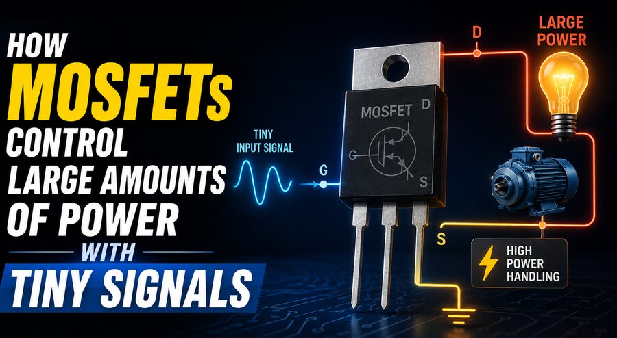

Modern electronics often need to solve an interesting problem: how can a tiny control signal switch or regulate a much larger amount of electrical power? 🔌⚙️
A microcontroller pin, for example, may produce only a few volts and a tiny amount of current. Yet that signal may ultimately control a motor drawing tens of amps, a power supply delivering hundreds of watts, or an inverter handling thousands of watts.
One of the most important devices that makes this possible is the MOSFET, short for Metal-Oxide-Semiconductor Field-Effect Transistor.
MOSFETs are found almost everywhere in modern power electronics, including:
- 💻 Computer power supplies
- 🚗 Electric vehicles
- ☀️ Solar inverters
- 🔋 Battery-management systems
- 🏭 Industrial motor drives
- 💡 LED lighting
- 📱 Phone chargers
- 🤖 Robotics
- ⚡ DC-DC converters
- 🖥️ Motherboards and processors
What makes MOSFETs remarkable is that a relatively small voltage applied to one terminal can control a much larger current flowing through two other terminals.
Understanding how this works reveals one of the most powerful ideas in electronics: using an electric field to control current without requiring continuous control current at the input.
🔌 What Is a MOSFET?
A MOSFET is a type of transistor used as either an electronic switch or an amplifying device.
A typical power MOSFET has three main electrical terminals:
- Gate (G) 🎛️
- Drain (D) ⚡
- Source (S) 🔌
Some MOSFETs also expose a fourth terminal called the body or bulk, although in many discrete power devices it is internally connected to the source.
The basic idea is simple.
The gate voltage controls whether current can flow between the drain and source.
In a commonly used N-channel enhancement MOSFET:
Low gate-to-source voltage → MOSFET mostly OFF
Sufficiently high gate-to-source voltage → MOSFET ON
This makes the MOSFET behave like a voltage-controlled electronic switch.
🎛️ Why Is the Gate So Important?
The gate is electrically insulated from the semiconductor channel by an extremely thin insulating layer.
In traditional silicon MOSFET terminology, this insulation is associated with silicon dioxide, which explains the “oxide” part of MOSFET.
Because the gate is insulated, ideally almost no steady-state current flows into it.
Instead, applying a voltage between the gate and source creates an electric field inside the transistor.
That electric field changes the conductivity of the semiconductor region beneath the gate.
This is the fundamental reason a tiny control circuit can command a much larger power path. ⚡
The control input does not need to continuously supply the same current that the load consumes.
🌊 How the Electric Field Creates a Conducting Channel
Consider an N-channel enhancement MOSFET.
When the gate-to-source voltage, written as VGS, is near zero, the device does not have a strongly conducting channel between drain and source.
The MOSFET is largely off.
As positive voltage is applied to the gate relative to the source, the resulting electric field attracts charge carriers into the region beneath the gate.
Once the gate voltage becomes sufficiently high, a conducting channel forms.
Current can then flow between drain and source.
The stronger the appropriate gate drive, within the device’s operating limits, the more strongly the channel can conduct.
This allows a small gate signal to control a much larger drain current. 🔄
⚠️ Threshold Voltage Does Not Mean Fully On
One common misunderstanding concerns a MOSFET specification called gate threshold voltage, or VGS(th).
The threshold voltage is approximately the point at which the MOSFET only begins to conduct a small specified current.
It does not normally mean the transistor is fully turned on.
Suppose a datasheet lists:
VGS(th) = 2 V to 4 V
That does not necessarily mean that 4 V is enough for efficient high-current operation.
The MOSFET may require a higher gate voltage—perhaps 10 V in a conventional device—to reach the low on-resistance specified elsewhere in the datasheet.
Special logic-level MOSFETs are designed to operate effectively with lower gate voltages such as 5 V or sometimes around 3.3 V, depending on the device.
Always check the datasheet’s specified RDS(on) at the intended gate voltage. 📄
🔋 How Can a Tiny Signal Control Huge Current?
This is the key question.
Imagine a microcontroller producing a 5 V control signal.
That signal may ultimately switch a MOSFET carrying:
20 A at 48 V
The switched load power could be:
Power = Voltage × Current
P = 48 × 20 = 960 W
Almost one kilowatt of power is being controlled by a tiny digital signal. ⚡
The important point is that the control signal is not supplying those 960 watts.
The load’s power comes from a separate power source.
The MOSFET simply controls whether that energy is allowed to flow through the circuit.
The gate signal is therefore more like a command than a source of load energy.
A useful analogy is a valve.
A small movement of a valve handle can control a large flow of water.
The handle does not supply the water—it controls the path.
Similarly, a MOSFET gate controls electrical current supplied by another source. 🚰➡️⚡
🚪 MOSFET as an Electronic Switch
Power MOSFETs are often operated in two main states:
🔴 OFF State
The gate voltage is below the required level.
The drain-to-source path has very high resistance.
Only tiny leakage currents ideally flow.
🟢 ON State
The gate is driven strongly enough.
The drain-to-source path becomes highly conductive.
The MOSFET behaves approximately like a low-value resistor.
This resistance is called:
RDS(on)
A good power MOSFET may have an on-resistance measured in only a few milliohms.
For example:
RDS(on) = 0.005 Ω
If 20 A flows through it, conduction loss can be estimated using:
P = I²R
So:
P = 20² × 0.005
P = 2 W
The MOSFET can therefore control hundreds of watts of load power while dissipating only a relatively small amount of heat itself, assuming suitable operating conditions.
That high efficiency is one reason MOSFETs dominate many switching applications. 🔥➡️❄️
🧠 Why MOSFETs Are Called Voltage-Controlled Devices
A bipolar junction transistor, or BJT, typically requires continuous base current to maintain conduction.
A MOSFET behaves differently.
Its gate is primarily controlled by voltage.
Once the gate is charged to the desired voltage, ideally very little DC current is needed to hold it there.
This gives MOSFETs very high input impedance.
However, saying that a MOSFET gate “draws no current” can be misleading.
During switching, the gate behaves much like a small capacitor.
Current is required to charge and discharge it.
That detail becomes extremely important at high switching frequencies. ⚡
🪫 The Gate Acts Like a Capacitor
The insulated gate structure creates capacitance.
To turn a MOSFET on, the control circuit must move electrical charge onto the gate.
To turn it off, that charge must be removed.
Datasheets often specify a parameter called total gate charge, usually written as Qg.
Suppose a MOSFET has:
Qg = 80 nC
If it is switched only once, this is a tiny amount of energy.
But if it switches tens or hundreds of thousands of times per second, repeatedly charging and discharging the gate requires significant current from the driver.
This is why high-power MOSFET circuits often use a dedicated gate-driver IC instead of connecting the MOSFET directly to a microcontroller.
🚀 What Does a Gate Driver Do?
A gate driver takes a low-power control signal and provides the larger, short-duration currents required to charge and discharge the MOSFET gate quickly.
For example, a microcontroller might provide:
3.3 V logic signal at a few milliamps
The gate driver may convert this into:
10 V gate drive with peak currents of several amps
The gate driver does not continuously feed several amps into the MOSFET.
Instead, it provides high current briefly during switching transitions.
This allows the MOSFET to move rapidly between OFF and ON states.
Fast switching reduces the time the device spends partially conducting, which can significantly reduce heat generation. 🔥
🌡️ Why Partially Turning On a MOSFET Creates Heat
When a MOSFET is completely off, very little current flows.
When it is fully on, the voltage across it may be very small.
In both cases, power loss can be relatively low.
The dangerous region is often the transition between those states.
Instantaneous power is:
P = V × I
Suppose during a switching transition the MOSFET temporarily has:
20 V across it
while carrying:
10 A
The instantaneous dissipation is:
200 W
This may occur only for a very short time, but repeated millions of times, those losses can become important.
Therefore, power-electronics designers try to switch MOSFETs quickly while managing electromagnetic interference and voltage/current overshoot.
🔁 Switching Losses vs Conduction Losses
A MOSFET typically experiences two major categories of power loss.
🔹 Conduction Loss
This occurs while the MOSFET is on.
It is approximately:
Pconduct ≈ I² × RDS(on)
Lower RDS(on) generally reduces conduction losses.
🔹 Switching Loss
This occurs during turn-on and turn-off transitions.
During these brief moments, the MOSFET may simultaneously experience substantial voltage and current.
Switching losses become more important as switching frequency increases.
Designers therefore choose MOSFETs based on trade-offs between:
- On-resistance
- Gate charge
- Voltage rating
- Current rating
- Switching speed
- Thermal performance
The MOSFET with the lowest RDS(on) is not automatically the best device for every application. ⚖️
📊 Pulse-Width Modulation Gives Fine Power Control
MOSFETs are not limited to simply turning a load permanently on or off.
They can switch extremely rapidly using Pulse-Width Modulation, or PWM.
Suppose a MOSFET controls a DC motor.
The controller might switch the MOSFET on and off thousands of times per second.
If the MOSFET is on 25% of the time, the motor receives less average energy.
At 75% duty cycle, it receives more.
This allows precise control of:
- Motor speed 🏎️
- LED brightness 💡
- Heater power 🔥
- Battery charging 🔋
- Power-converter output ⚡
The MOSFET itself spends most of its time either fully on or fully off, helping maintain high efficiency.
💡 Example: Controlling a High-Power LED
Imagine a 100 W LED lighting system.
A microcontroller cannot directly power the LED.
Its output pin may be capable of only a few tens of milliamps.
Instead:
Microcontroller → Gate Driver → MOSFET → LED Power Circuit
The microcontroller generates a tiny PWM signal.
The MOSFET repeatedly switches the much larger LED current.
Changing PWM duty cycle changes perceived brightness.
Thus a low-power digital signal controls a high-power lighting system with excellent efficiency. 💡⚡
🚗 MOSFETs in Electric Vehicles
Electric vehicles use power semiconductor devices throughout their electrical systems.
MOSFETs are especially common in lower- and medium-voltage subsystems such as:
- Battery management
- DC-DC converters
- Pumps
- Fans
- Lighting
- Electronic control modules
- Power distribution
High-performance power systems may use silicon MOSFETs, silicon-carbide MOSFETs, IGBTs, or other devices depending on voltage and power requirements.
Silicon-carbide MOSFETs are increasingly important because they can offer fast switching and high efficiency at high voltages. 🚗🔋
☀️ MOSFETs in Solar Power Systems
Solar panels generate DC electricity, while homes and power grids commonly use AC.
An inverter converts the panel’s DC energy into controlled AC power.
Power transistors repeatedly switch currents through inductors, transformers, and filter networks.
MOSFETs and related power semiconductors make this conversion possible at high efficiency.
A small digital controller determines the switching pattern.
The MOSFETs then control much larger currents from the solar array.
Once again:
Tiny information signal → enormous controlled energy flow ☀️⚡
🔄 The Body Diode
Power MOSFETs contain an intrinsic structure that behaves like a diode between source and drain.
This is commonly called the body diode.
It becomes especially important when switching inductive loads such as:
- Motors
- Solenoids
- Transformers
- Inductors
Inductors resist sudden changes in current.
When a MOSFET switches, the stored magnetic energy needs somewhere to go.
Depending on circuit topology, the body diode may provide a temporary current path.
However, its electrical characteristics may not always be ideal, so designers sometimes add external diodes or use carefully coordinated synchronous switching.
🧲 Why Inductive Loads Are Challenging
A motor winding behaves partly like an inductor.
When current flows through it, energy is stored in a magnetic field.
If the MOSFET suddenly interrupts the current, the inductor attempts to keep that current flowing.
This can produce a large voltage spike. ⚡📈
Without protection, the spike may exceed the MOSFET’s drain-to-source voltage rating and damage it.
Designers may use:
- Flyback diodes
- Snubber circuits
- TVS diodes
- Clamp networks
- Controlled switching techniques
Protecting MOSFETs from inductive transients is one of the most important practical considerations in power electronics.
🌡️ Why MOSFETs Need Heat Sinks
Even highly efficient MOSFETs generate heat.
A transistor dissipating only 5 W may become extremely hot if that heat cannot escape.
MOSFETs have specified thermal parameters describing how easily heat travels from the semiconductor junction to the case and surrounding air.
High-power designs may use:
- Aluminum heat sinks
- Cooling fans
- Thermal pads
- Copper PCB areas
- Liquid cooling
- Heat spreaders
Keeping junction temperature within safe limits is essential for reliability. 🌡️
Excessive temperature can increase electrical losses and shorten component lifetime.
📈 Why RDS(on) Changes With Temperature
A MOSFET’s on-resistance is not constant.
For many silicon power MOSFETs, RDS(on) increases as junction temperature rises.
Suppose a device has an RDS(on) of 5 milliohms at room temperature.
At high operating temperature, that resistance may become significantly larger.
Because conduction loss is proportional to resistance:
More temperature → more resistance → more heat
This creates an important thermal feedback effect.
Designers must use the datasheet’s temperature curves rather than assuming the room-temperature specification always applies.
⚡ Voltage Rating Matters
Every MOSFET has a maximum drain-to-source voltage rating, commonly written as VDS.
A 60 V MOSFET should not be used casually in a circuit where voltage spikes may approach or exceed 60 V.
Designers generally provide sufficient margin for:
- Power-supply variation
- Inductive spikes
- Switching transients
- Noise
- Abnormal operating conditions
Using insufficient voltage margin can cause avalanche breakdown or catastrophic failure.
Higher voltage ratings, however, often come with trade-offs such as higher on-resistance.
Device selection therefore requires balance. ⚖️
💪 Current Ratings Can Be Misleading
Datasheets may advertise extremely high current ratings.
A MOSFET might appear capable of carrying 100 A or more.
However, that number is often based on very specific test conditions, such as an ideal case temperature.
Real-world current capability may be limited by:
- Package leads
- PCB copper thickness
- Connectors
- Heat sinking
- Junction temperature
- RDS(on)
- Switching losses
Engineers should not select a MOSFET based only on the large current number printed on the datasheet.
Thermal calculations and realistic operating conditions matter much more. 📐
🔗 Putting MOSFETs in Parallel
For extremely high current, designers can place multiple MOSFETs in parallel.
If current shares evenly, each transistor carries only part of the total load.
This can reduce total conduction resistance.
For example, two identical MOSFETs with approximately equal current sharing can provide roughly half the effective on-resistance of one device.
However, practical parallel operation requires careful layout.
Unequal gate-drive paths, thermal differences, and PCB resistance can cause one MOSFET to carry more current than another.
Good engineering is still required. 🔧
🔼 High-Side and Low-Side Switching
MOSFETs can be positioned in different places relative to the load.
🔹 Low-Side Switch
The MOSFET sits between the load and ground.
This is often straightforward because the source is near ground potential.
🔹 High-Side Switch
The MOSFET sits between the power supply and the load.
High-side switching can require more sophisticated gate-drive circuitry, especially with N-channel MOSFETs.
In bridge circuits, designers may use dedicated high-side/low-side gate drivers.
These are fundamental building blocks of motor controllers and power converters.
🌉 The H-Bridge
An H-bridge typically uses four switching devices arranged around a load such as a motor.
By controlling which MOSFETs are on, current can flow through the motor in either direction.
This allows:
- Forward rotation
- Reverse rotation
- Electronic braking
- PWM speed control
H-bridges are widely used in robotics, electric actuators, drones, and motor-control systems. 🤖
However, the control system must prevent both MOSFETs on the same bridge leg from conducting simultaneously.
💥 What Is Shoot-Through?
Suppose the high-side and low-side MOSFET in the same half-bridge turn on together.
They create a very low-resistance path directly from the positive supply to ground.
This condition is called shoot-through.
The resulting current can be enormous and may destroy the transistors almost instantly. 💥
Gate drivers therefore introduce a short delay called dead time between switching one transistor off and turning the opposite transistor on.
Careful dead-time control is essential in efficient bridge converters.
⚡ MOSFETs in Switching Power Supplies
Most modern chargers and power supplies use switching conversion instead of wasting energy with linear regulation.
A MOSFET rapidly switches electrical energy into an inductor or transformer.
A controller measures the output voltage and adjusts the switching pattern.
Common converter types include:
- Buck converters ⬇️
- Boost converters ⬆️
- Buck-boost converters 🔄
- Flyback converters
- Full-bridge converters
- Resonant converters
The transistor can switch tens of thousands or even millions of times per second.
Because it operates mostly in efficient ON and OFF states, very high conversion efficiency becomes possible.
📱 Why Chargers Have Become Smaller
Older power adapters often relied on low-frequency transformers, which were large and heavy.
Modern switch-mode power supplies operate at much higher frequencies.
Higher-frequency switching allows the use of smaller transformers, inductors, and capacitors.
Fast MOSFETs are a major reason this is possible.
New semiconductor materials such as gallium nitride (GaN) can switch even faster than many conventional silicon devices.
That is one reason modern high-power phone and laptop chargers can be surprisingly compact. 📱🔌
💎 Silicon Carbide and Gallium Nitride
Traditional MOSFETs are mainly made from silicon.
Newer power-electronics technologies increasingly use wide-bandgap semiconductor materials.
🔹 Silicon Carbide — SiC
SiC MOSFETs can be especially useful for high-voltage, high-temperature, and high-efficiency applications.
They are increasingly used in:
- EV inverters
- Fast chargers
- Solar systems
- Industrial power conversion
🔹 Gallium Nitride — GaN
GaN power transistors can offer extremely fast switching and low switching losses.
They are increasingly found in compact chargers and high-frequency converters.
Both technologies continue the same fundamental idea: using a small control signal to manage large amounts of electrical energy efficiently. ⚡
🔐 Gate Voltage Has Limits Too
Although the MOSFET gate is insulated, it is not indestructible.
The thin gate dielectric can be damaged if excessive voltage is applied.
Datasheets specify a maximum gate-to-source voltage, often written as:
VGS(max)
A common value for some silicon power MOSFETs is approximately ±20 V, although the actual specification varies.
Electrostatic discharge can also damage the gate.
This is why proper handling and gate protection are important.
Designers may use:
- Gate resistors
- Zener clamps
- Driver protection
- Careful PCB layout
to protect the device. 🛡️
🧮 A Simple Power-Control Example
Suppose a MOSFET controls a 12 V heating element drawing 15 A.
The load power is:
Pload = 12 × 15 = 180 W
Now suppose the MOSFET’s RDS(on) is:
0.01 Ω
Its approximate conduction loss is:
PMOSFET = I²R
PMOSFET = 15² × 0.01
PMOSFET = 2.25 W
So the transistor is controlling roughly 180 W of load power while dissipating only around 2.25 W from conduction, before considering switching and other losses.
The gate-control circuit itself may require only tiny average power.
This illustrates how efficiently MOSFETs separate the control path from the power path.
🧠 The Deeper Principle
A MOSFET does not magically create power.
It controls energy supplied from somewhere else.
The gate signal changes an electric field inside the semiconductor.
That field changes the resistance of the drain-to-source path.
The load’s power supply then provides the large current.
This distinction is essential:
The gate provides information and control.
The power source provides energy.
That separation is the reason tiny electronic controllers can command powerful machines. 🎛️➡️🏭
🚀 Final Thoughts
MOSFETs are among the most important components in modern electronics because they allow small voltage signals to control enormous electrical power efficiently and rapidly.
Their insulated gate creates an electric field that controls conductivity between the drain and source. Because very little steady-state gate current is required, even low-power digital electronics can command high-current circuits through suitable gate drivers.
When used as switches, MOSFETs can achieve remarkably low losses because they spend most of their time either:
OFF with almost no current, or
ON with very low resistance.
This makes them ideal for switching power supplies, motor controllers, LED drivers, solar inverters, battery systems, electric vehicles, and countless other technologies. ⚡
Their true strength becomes even clearer when PWM is added. A microcontroller producing only a tiny digital waveform can regulate motor speed, converter voltage, battery charging, or lighting power by switching a MOSFET thousands of times per second.
Of course, real power electronics requires careful attention to gate charge, switching losses, heat dissipation, voltage spikes, device ratings, dead time, and circuit layout. A MOSFET may be easy to turn on in a simple experiment, but controlling hundreds or thousands of watts reliably requires thoughtful engineering.
Still, the underlying concept remains beautifully simple:
A tiny electrical signal changes an electric field, the electric field opens or closes a conductive path, and that path controls a much larger flow of electrical energy. 🎛️⚡
That ability to separate a low-power control signal from a high-power energy path is why MOSFETs have become fundamental building blocks of the modern electrical world—from the charger in your pocket to the power electronics inside an electric vehicle. 🔋🚗✨