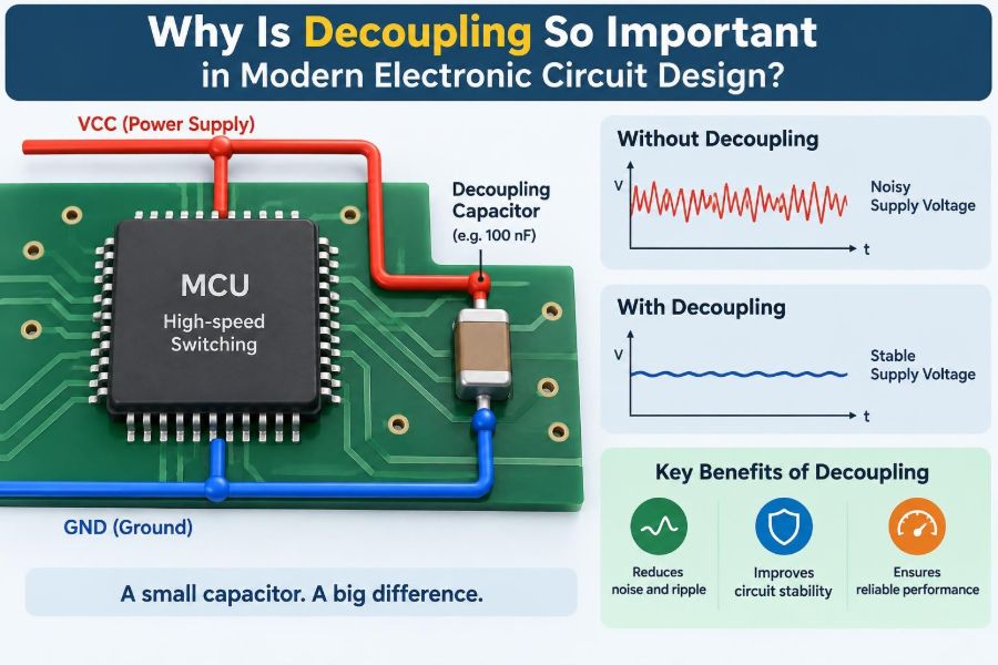

A microcontroller board works perfectly on the bench, then resets the moment a motor starts. An audio circuit develops a faint digital whine. A fast sensor interface reports occasional values that make no physical sense. These failures can seem unrelated, yet they often have the same root cause: the power rail is not as stable as the schematic suggests.
On a circuit diagram, power symbols imply a clean, fixed voltage available everywhere. On a real PCB, power travels through traces, vias, connectors, planes, and components that all have resistance, inductance, and capacitance. Every switching event disturbs that path.
Decoupling capacitors provide local energy and a controlled path for high-frequency current. They are small, inexpensive parts, but their placement and selection affect whether a modern circuit starts reliably, communicates cleanly, meets noise limits, and behaves predictably.
Understanding decoupling is not just about memorising “put a 100 nF capacitor at every IC.” It is about understanding current loops, frequency, physical layout, and the limitations of real components.
🔋 What Decoupling Actually Means
Decoupling is the practice of preventing one part of a circuit from disturbing another through a shared power supply or ground connection. A decoupling capacitor is connected between a supply rail and its return path, usually ground, close to the load that creates changing current demand.
The capacitor temporarily supplies or absorbs current when the load changes faster than the upstream power network can respond. This reduces local voltage movement and keeps switching noise from spreading across the board.
⚡ Why Digital Circuits Demand Pulses of Current
Logic ICs do not draw a perfectly steady current. CMOS gates consume much of their dynamic current while internal transistors change state and while output pins charge or discharge capacitance.
A processor may therefore draw short, sharp current pulses at clock edges, bus transitions, and internal activity bursts. Even a device whose average current is modest can have demanding instantaneous current requirements.
The regulator and bulk capacitor may be capable of supplying the average load. The challenge is delivering current at the exact location and timescale where it is needed.
🌊 The Supply Rail Is a Network, Not an Ideal Source
An ideal voltage source holds its output constant regardless of load current. Real supplies cannot do that at every frequency. Cable resistance, regulator control-loop bandwidth, PCB trace impedance, and connector inductance all limit the response.
At low frequencies, a regulator can adjust its output. At higher frequencies, energy must come from capacitors. At very high frequencies, the capacitor has to be physically close enough that the connection itself does not dominate.
📉 The Voltage-Droop Relationship
Two simple relationships explain much of decoupling design. Capacitor charge storage gives ΔV = IΔt/C: if a load draws extra current for a time interval, a larger capacitance produces less voltage droop.
But a fast current change also creates a voltage step through inductance: V = L(di/dt). This is why capacitance alone is not enough. A physically distant 100 µF capacitor can be ineffective for a very fast edge because the path inductance produces a large transient voltage before the capacitor can help.
🧭 Current Loops Matter More Than Schematic Distance
A useful mental model is to trace the loop. During a fast switching event, current leaves the local decoupling capacitor, enters the IC power pin, returns through a ground pin or plane, and arrives back at the capacitor.
The area enclosed by that loop should be as small as practical. A small loop has lower inductance, radiates less electromagnetic energy, and creates less voltage disturbance. The capacitor may look close on a schematic while being electrically far away on the PCB.
📍 Why Capacitor Placement Is So Critical
Place the smallest high-frequency decoupling capacitor close to the relevant power pin, with a short, wide connection to the power and ground network. For surface-mount parts, this often means placing it beside the pin rather than somewhere along the same rail.
A ground via located immediately near the capacitor pad can be valuable when using a ground plane. Routing the capacitor through a long trace to a remote via adds inductance to the very loop the capacitor is meant to control.
🧱 PCB Inductance Can Defeat Good Intentions
Inductance is not restricted to coils. Every trace, via, component termination, and plane transition contributes some inductance. At fast edge rates, even very short interconnects matter.
This explains a common surprise: moving a capacitor only a few millimetres can substantially change ringing or supply noise. The difference is not magic; it is a changed current-loop geometry.
🧪 Real Capacitors Are Not Ideal Capacitors
An ideal capacitor has only capacitance. A real one also has equivalent series resistance (ESR) and equivalent series inductance (ESL). ESR causes voltage drop and dissipation when current flows. ESL limits high-frequency usefulness.
The effective impedance is therefore frequency dependent. As frequency rises, capacitive impedance falls until the capacitor reaches its self-resonant frequency. Beyond that point, ESL makes its behaviour increasingly inductive.
🎼 Self-Resonance Explains Frequency Limits
At self-resonance, the capacitor’s capacitive and inductive effects cancel, giving its lowest impedance. This is often the region where it is most effective at shunting noise.
Above self-resonance, adding more of the same component at the same location may not solve a high-frequency problem. Package size, mounting geometry, and layout can matter as much as the nominal capacitance printed on a bill of materials.
📦 Package Size Changes High-Frequency Performance
Smaller multilayer ceramic capacitor packages generally have lower parasitic inductance than larger packages, all else equal. That can make a smaller capacitor effective at higher frequencies even if its nominal capacitance is lower.
This is not a universal rule to choose the smallest part everywhere. Voltage rating, available capacitance, assembly capability, reliability requirements, and DC-bias behaviour must also be considered. It is a reminder that a capacitor is an RF component as well as an energy-storage component.
🪜 Why Designs Use Multiple Capacitance Values
A power distribution network normally needs support across a broad frequency range. Larger capacitors help with slower load changes and regulator stability; local ceramics handle faster demand near IC pins.
A practical arrangement might include bulk capacitance near a regulator or power entry, moderate local capacitance for IC groups, and small ceramics beside individual power pins. The exact values should come from the device data sheet, load behaviour, and layout constraints rather than a fixed recipe.
⚠️ More Values Are Not Always Better
It is tempting to scatter 10 µF, 1 µF, 100 nF, and 10 nF capacitors around every supply pin. That approach can work in uncomplicated boards, but it is not automatically optimal.
Capacitors and interconnect inductance can form resonances. Mixed values may introduce impedance peaks, sometimes called anti-resonances, at frequencies where the supply network performs worse. For sensitive or high-current rails, simulation or measurement is more reliable than folklore.
🏷️ Read the IC Data Sheet First
Many IC manufacturers provide required or recommended capacitors, placement guidance, and sometimes PCB examples. These recommendations may include specific values, dielectric types, ESR ranges, or separate capacitors for analogue, digital, core, and input/output rails.
Such instructions are often tied to internal regulator stability, converter operation, or measured switching behaviour. Treat required capacitors and placement notes as functional design constraints, not as optional tidy-up components.
🧠 Decoupling Versus Bypass Versus Bulk Capacitors
These terms overlap in everyday engineering conversation, but the distinctions are useful. A bypass capacitor provides a low-impedance path that diverts unwanted AC noise away from a node. A decoupling capacitor isolates local load transients from the wider supply network.
A bulk capacitor stores relatively large energy for slower variations, cable effects, or load steps. One physical capacitor can serve more than one role, but assigning a purpose helps when choosing value, location, and technology.
| Type | Main job | Typical location | Useful timescale |
|---|---|---|---|
| Local ceramic | Fast local current loop | At an IC supply pin | Fast edges and high frequencies |
| Mid-range capacitor | Support a local rail region | Near an IC cluster or converter | Intermediate transients |
| Bulk capacitor | Energy storage and slower load steps | Power entry or regulator output | Lower-frequency changes |
🏭 Ceramic Capacitors and DC Bias
High-value ceramic capacitors commonly use Class II dielectrics such as X5R or X7R. Their actual capacitance can fall significantly under applied DC voltage, and it can also vary with temperature and ageing.
A part marked 10 µF may not provide 10 µF in its intended circuit. Check the manufacturer’s capacitance-versus-bias curves, especially on low-voltage rails where a small package is operated close to its voltage rating.
🌡️ Dielectric Choice Affects Stability
Class I ceramic dielectrics, such as C0G/NP0, are highly stable but are generally available in smaller capacitances. They are excellent where predictable capacitance, low loss, or low distortion is needed.
Class II ceramics offer much greater capacitance per volume but change more with conditions. Electrolytic and polymer capacitors provide useful bulk energy and damping characteristics, though their ESR, lifetime, and frequency behaviour differ. The best technology depends on the rail’s actual needs.
🔌 Regulators Need Their Own Capacitors
Linear regulators and switching regulators are control systems. Input and output capacitors influence their stability, transient response, ripple, and conducted emissions. A regulator data sheet may specify a minimum capacitance, an ESR range, or an allowed capacitor family.
Putting a large capacitor “somewhere on the board” is not equivalent to placing the required components at the regulator pins. Long input paths can also let a switching converter inject ringing back into its supply connection.
🔄 Switching Converters Create Fast, High-Current Loops
In a buck converter, the input capacitor must handle pulsed current from the switching action. It belongs very close to the switching MOSFET and return path identified by the converter layout guidance.
The output capacitor similarly controls output ripple and load response, but it is part of a different loop. Poor placement can increase ringing, reduce efficiency, create EMI problems, or stress components even when the schematic is correct.
📡 Decoupling Helps Control EMI
A noisy power loop can act as an antenna. Rapidly changing current in a large loop produces magnetic fields; voltage ringing can excite traces and cables. Good decoupling reduces the size and energy of these disturbances at their source.
It is not a substitute for complete electromagnetic compatibility design. Return-path continuity, edge-rate control, shielding, filtering, connector treatment, and enclosure design may all be necessary. Still, local decoupling is one of the most effective first defences.
🎧 Sensitive Analogue Circuits Need Quiet Returns
Operational amplifiers, ADC references, RF blocks, and precision sensors can be affected by supply noise that digital logic barely notices. Noise may appear as offset movement, reduced measurement resolution, spurious tones, or degraded receiver sensitivity.
Local capacitors should follow the component manufacturer’s guidance, often using a small ceramic near each supply pin and suitable local bulk support. The return path must be planned carefully: separating noisy current loops is usually more useful than simply splitting ground planes without understanding where return current flows.
🧩 Mixed-Signal Boards Need Intentional Partitioning
A mixed-signal board combines noisy digital switching with circuits that may measure microvolt- or millivolt-level signals. Partition components so high-current digital and converter loops do not cross sensitive analogue regions.
Use the converter or ADC data sheet to determine how analogue and digital supplies should be filtered or joined. A ferrite bead can be useful in some cases, but it is not a universal fix; its impedance, DC current rating, and interaction with capacitors need consideration.
🖥️ Every Power Pin Is a Design Clue
Modern ICs often provide multiple power and ground pins because current must enter and return at several locations within the package. Omitting capacitors on “extra” supply pins because the pins share a net can lead to poor local power integrity.
As a starting point, follow the stated requirement for each pin or pin group. Multi-rail processors, FPGAs, memory devices, and high-speed interfaces may have especially detailed power-distribution recommendations.
🧷 Ground Pins Are Half of the Decoupling System
A decoupling capacitor cannot work well without a low-inductance return path. The capacitor’s ground terminal, the IC ground pin, and the ground plane connection must form a compact loop.
Ground is not a magical zero-voltage point. A shared return path has impedance, so current from one circuit can create a voltage disturbance seen by another. This is one reason solid, continuous reference planes are so valuable.
🛠️ A Practical Placement Workflow
Start placement with the parts whose loops are most critical: switching regulators, high-speed processors, clocks, memory, RF devices, and precision converters. Put their required capacitors down before routing less sensitive circuitry.
- Identify every supply rail, current level, and device-specific capacitor requirement.
- Place pin-level ceramics adjacent to their associated power pins.
- Provide a short return into a continuous ground reference plane.
- Add bulk and regional capacitance near regulators and load clusters.
- Review the actual current loops on every copper layer, not just component proximity.
- Check that routing, vias, and mechanical constraints have not forced critical capacitors away from their pins.
🔍 Common Layout Mistakes
- Placing all capacitors in a neat row far from the IC for visual tidiness.
- Connecting capacitor pads through narrow, long traces.
- Using one shared via for several high-frequency capacitor returns.
- Breaking the ground plane beneath a fast signal or decoupling loop.
- Assuming one large bulk capacitor can replace local ceramics.
- Ignoring the actual capacitance of biased Class II ceramics.
These mistakes are common because a schematic can hide physical parasitics. PCB layout is part of the electrical design, not merely its packaging.
📏 Estimating Capacitance Without False Precision
The relation C ≥ IΔt/ΔV can provide an initial estimate for capacitance needed during a transient. For example, it can help frame whether a rail needs microfarads or hundreds of microfarads to bridge the interval before a regulator responds.
However, the estimate does not capture capacitor ESR, ESL, control-loop response, package inductance, changing load profiles, or plane impedance. Use it as a sizing clue, then validate the assembled system.
📊 Impedance Is the Real Design Target
A rail has a voltage-noise budget and a changing current demand. Their ratio suggests a target impedance: approximately Ztarget = ΔV/ΔI. The power distribution network should remain below that impedance across the frequency range that matters.
This framing is particularly useful for demanding digital rails because it shifts the question from “How many capacitors?” to “Is the rail impedance low enough where the load needs it?” It also reveals why placement and planes are inseparable from component values.
🧰 Simulation Can Expose Resonances Early
Power-integrity tools can model capacitor parasitics, plane structures, package models, and regulator behaviour. Even a simplified impedance plot can expose a resonance peak or show that a chosen capacitor loses effectiveness above a relevant frequency.
Models have limits, and results are only as credible as their inputs. They are most useful for comparing options, guiding layout choices, and identifying risks that deserve measurement on hardware.
🔬 Measuring Decoupling in the Lab
Oscilloscope probing can easily create misleading results. A standard long ground clip adds inductance and may display ringing caused mainly by the probe loop. Use a short ground spring, coaxial probing method, or a suitable probe adapter when checking high-frequency rail noise.
Measure close to the load and compare operating conditions: idle versus active processing, radio transmission, motor start-up, or peak communication traffic. For deeper analysis, a network analyser or specialised power-integrity measurement approach may be appropriate.
🚦 Symptoms of Inadequate Decoupling
Possible symptoms include unexplained resets, intermittent communication errors, clock instability, ADC noise, excessive supply ripple, radiated-emissions failures, or behaviour that changes when a probe touches the board.
None of these symptoms proves decoupling is at fault. Firmware defects, poor grounding, regulator instability, signal-integrity problems, and faulty components can look similar. The useful response is to form a hypothesis, inspect the current loop, and measure before changing parts at random.
🧯 When Extra Capacitance Causes Trouble
Additional capacitance can increase inrush current, slow power sequencing, alter a regulator’s transient response, or violate a regulator’s stability requirements. Large ceramics can also create mechanical or acoustic effects in some applications.
For hot-plugged systems, battery-powered devices, and tightly controlled startup rails, capacitor additions should be assessed with the power-source capability and sequencing requirements in mind.
🏁 A Reliable Decoupling Design Mindset
Good decoupling begins by asking where current comes from during a fast event and how it returns. It then matches capacitor technology, value, and placement to that loop and to the timescale of the load transient.
The central principle is simple: keep fast transient current local, make its loop short and low inductance, and let the wider supply handle slower energy delivery. Data-sheet guidance, continuous reference planes, realistic component models, and careful measurement turn that principle into a reliable board.
Decoupling is important because stable electronics depend not only on having the right voltage, but on delivering the right current through the right physical path at the right instant. Treat every capacitor as part of a current loop, and many “mysterious” hardware problems become understandable—and preventable. 🔌📐⚡