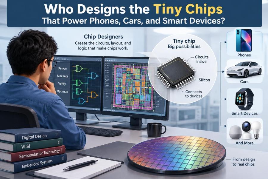

Your phone wakes you with an alarm, connects to a network, captures images, manages battery charging, and renders a map—all through chips too small to notice. A modern car does something similarly complex: it measures wheel speed, controls motor or engine functions, runs displays, and assists the driver with a growing collection of electronic systems.
These chips do not appear as finished objects from a single inventor’s desk. They are the outcome of a large engineering process that turns an idea into billions of precisely arranged transistors, then into a reliable product operating in a hot pocket, a vibrating car, or a wireless sensor.
The people who make that possible are broadly called integrated-circuit (IC) designers, chip designers, or semiconductor engineers. But those titles cover many specialized roles, from defining what a chip should do to checking that every microscopic connection can be manufactured.
Understanding who designs chips also explains why electronics engineering combines circuit theory, programming, physics, verification, manufacturing knowledge, and careful teamwork. The tiny silicon die is only the visible center of a much bigger system.
🔍 What Counts as a Chip?
A chip, formally an integrated circuit, is an electronic circuit fabricated on a small piece of semiconductor material, usually silicon. Rather than wiring individual transistors, resistors, and capacitors together on a circuit board, engineers create enormous numbers of components and interconnections in layers on one die.
Chips range from simple power-management devices to processors containing many functional blocks. A phone may contain separate chips for computing, cellular communication, memory, charging, Wi-Fi, display control, sensors, and audio.
🧠 The Broad Answer: IC Design Teams
There is rarely one person who “designs the chip.” An IC design team brings together engineers with distinct responsibilities and reviews each other’s work repeatedly.
At a high level, the team translates a product need into an electrical specification, a digital or analog implementation, a physical layout, and finally data that a fabrication facility can use. Product, test, packaging, software, and applications engineers continue the work after the silicon arrives.
📋 Product Architects Define the Job
Chip architects decide what the device must accomplish and what trade-offs are acceptable. For example, a wearable processor may prioritize low energy use and compact memory, while an automotive controller may prioritize predictable behavior, long-term availability, diagnostics, and operation over a wide temperature range.
They set high-level requirements such as interfaces, performance targets, memory capacity, power limits, safety features, and approximate cost. A vague requirement such as “make it faster” is not enough; engineering needs measurable conditions and realistic constraints.
🧩 System Engineers Divide a Complex Problem
System engineers turn the architecture into connected blocks. A chip for a smart speaker might include processor cores, memory controllers, audio interfaces, security hardware, clock generation, and power-control logic.
This partitioning matters because blocks must exchange data correctly, share clocks safely, and stay within a power budget. An elegant block design can still fail at system level if its assumptions about timing, reset behavior, or data format do not match its neighbors.
💻 Digital Designers Build Logic from RTL
Digital IC designers describe hardware behavior using a hardware description language such as Verilog, SystemVerilog, or VHDL. The resulting register-transfer level, or RTL, specifies how data moves between registers and what logic transforms it on each clock cycle.
RTL resembles code, but it is not ordinary software. It describes circuitry that can operate in parallel. A designer must think about clock edges, bit widths, timing paths, reset states, and what physical hardware the description will become.
⚡ Analog Designers Shape Continuous Signals
Many real-world signals are continuous rather than binary. Analog IC designers create circuits that manage voltage, current, noise, frequency, amplification, filtering, and regulation.
Examples include microphone preamplifiers, voltage references, battery chargers, radio-frequency sections, data converters, and sensor interfaces. Analog work is sensitive to device behavior, parasitic effects, temperature, and manufacturing variation, so simulation and layout discipline are especially important.
🔀 Mixed-Signal Design Connects Two Worlds
Mixed-signal chips combine analog and digital functions. An analog-to-digital converter, for instance, samples a physical voltage and produces digital numbers that a processor can use.
The boundary is challenging. Fast digital switching can inject noise into sensitive analog circuitry through supply lines, the substrate, or nearby interconnect. Designers use partitioning, filtering, shielding, careful grounding strategies, and dedicated power domains to manage those interactions.
📡 RF Engineers Make Wireless Links Possible
Radio-frequency, or RF, IC engineers design circuits that operate at high frequencies for functions such as Bluetooth, Wi-Fi, cellular communication, satellite reception, and radar. They work with amplifiers, mixers, oscillators, filters, and impedance-matching networks.
At RF frequencies, a wire is no longer just a simple connection. Its geometry and surroundings affect behavior. Package, circuit-board, and antenna design may all influence the final wireless performance, which makes cross-disciplinary collaboration essential.
🧮 Memory Designers Solve a Different Density Problem
Memory chips store data using repeated cells arranged in large arrays. Engineers optimize these cells for density, speed, energy use, retention, and reliable read/write operation.
Not all memory serves the same role. Volatile memory temporarily holds working data, while nonvolatile memory retains information without power. Embedded memory inside a processor and standalone memory devices also impose different design and manufacturing choices.
🛡️ Hardware Security Designers Protect Trust
Security hardware can store cryptographic keys, generate random values, authenticate software, and isolate sensitive operations. Its purpose is not simply to add a lock; it establishes a trustworthy starting point for the wider system.
Security design must consider both logical attacks and physical behavior. Fault injection, side-channel leakage, insecure debug access, and poorly managed key provisioning are examples of risks that require specialized analysis. Security features also need usable lifecycle processes, not only clever circuitry.
✅ Verification Engineers Ask “Does It Really Work?”
Verification engineers test whether the design meets its intended behavior before fabrication. They build simulations, testbenches, assertions, coverage plans, and sometimes formal checks that examine properties mathematically within defined limits.
Verification is a major part of digital chip development because finding an error after manufacture can be expensive or impossible to repair. The objective is not merely to run a few successful tests; it is to expose unusual sequences, conflicting requests, and corner conditions.
🧪 Why Corner Cases Matter So Much
A chip may work in its most common scenario and still fail when power arrives slowly, a reset occurs during a transfer, two requests happen together, or a buffer becomes full. These are called corner cases because they sit at the edges of normal operation.
Consider a hypothetical door-lock controller: it must define what happens if a wireless command arrives at the same instant as a low-battery warning and a reboot. Clear priorities and testable behavior make the design safer than assumptions left unstated.
⏱️ Timing Engineers Protect the Clock Budget
Digital circuits do not operate correctly merely because their Boolean logic is correct. Signals must reach destination registers in time relative to the clock. Static timing analysis checks large numbers of paths without trying every possible input sequence in simulation.
Timing closure is the process of adjusting logic, constraints, placement, clock networks, and sometimes architecture until required timing is met. Faster clocks are not free: they can increase power use, worsen signal integrity challenges, and reduce timing margin.
📐 Physical Design Turns Logic into Geometry
Physical design engineers transform a synthesized digital netlist into a physical implementation. They plan where major blocks sit on the die, place standard cells, build power networks, route interconnections, and construct clock distribution.
The layout must balance area, congestion, timing, heat, power delivery, and manufacturability. A chip can contain immensely long total interconnect length, so the route between two blocks may matter as much as the logic inside them.
🗺️ Layout Engineers Draw What Will Be Fabricated
For custom analog, RF, memory, and specialized digital blocks, layout engineers create the precise geometric patterns for transistors and metal layers. This is not decorative drawing. Spacing, symmetry, matching, shielding, and proximity influence electrical behavior.
Analog layouts often use mirrored or common-centroid arrangements to reduce mismatch caused by gradients across a die. The exact techniques depend on the circuit and process, but the principle is consistent: physical structure affects circuit performance.
🏭 Process Engineers Make Silicon a Usable Platform
A semiconductor process defines the layers, transistor structures, materials, and design rules available to the chip team. Process and device engineers develop and control the manufacturing technology used by a fabrication facility.
IC designers work within a process design kit, which includes transistor models, layout rules, libraries, and verification information. They do not independently choose every microscopic material step; they design for the capabilities and limits of a qualified process.
🏗️ Foundries Manufacture the Design
A foundry is a company or facility that manufactures semiconductor wafers for its customers or affiliated design groups. A chip design company may be “fabless,” meaning it focuses on design and relies on an external foundry for fabrication.
Manufacturing uses repeated deposition, patterning, etching, doping, and cleaning steps to build structures layer by layer. Design teams send final layout data, but fabrication success also depends on the process, masks, equipment control, and yield learning.
📦 Packaging Engineers Make a Die Into a Component
The bare die must be protected and connected to the outside world. Packaging engineers choose or develop packages that provide electrical connections, mechanical protection, thermal paths, and sometimes multiple dies in one assembly.
A package affects signal speed, heat removal, size, cost, and reliability. Advanced assemblies may place logic, memory, and other dies close together, improving bandwidth or reducing board area, but they add integration and thermal challenges.
🌡️ Thermal and Power Engineers Manage Real Limits
Every active chip dissipates some power as heat. If heat cannot leave the package and system effectively, temperature rises, leakage may increase, performance may be reduced, and long-term reliability can suffer.
Power integrity is equally practical. A circuit needs a stable supply voltage during rapid current changes. Designers analyze power grids, decoupling capacitance, voltage drop, and switching noise because an ideal supply on a schematic is not guaranteed on a real die.
🧫 Test Engineers Separate Good Devices from Defects
After wafer fabrication, automated test equipment applies patterns and measures each die or packaged component. Test engineers develop methods that identify manufacturing defects and confirm key specifications efficiently.
Testing occurs at more than one stage in many flows. Some tests screen dies on the wafer, while later tests check packaged parts. The goal is not to prove every imaginable behavior forever; it is to provide appropriate confidence and remove parts that do not meet defined requirements.
📈 Yield Engineers Improve What Can Be Shipped
Yield is the portion of manufactured devices that meet requirements. Yield engineers analyze test data and manufacturing information to find recurring failure patterns, then work with design, process, and test teams on corrective actions.
Yield is not just a factory concern. A layout that is unusually sensitive to variation, a difficult-to-test feature, or an inadequate design margin can affect how many usable parts result from a wafer.
🚗 Why Automotive Chips Need Extra Discipline
Automotive electronics may face temperature swings, vibration, electrical transients, long service lives, and consequences that differ sharply depending on the application. A cabin-light controller and a system related to propulsion or braking do not carry the same risk profile.
Engineering teams therefore pay close attention to requirements traceability, diagnostics, failure behavior, qualification plans, and system-level safety processes where applicable. No individual chip feature makes a system automatically safe; safety depends on the complete design and its intended use.
🔋 Why Battery Devices Favor Efficiency
For a wireless earbud, tracker, or sensor node, energy use often determines user experience more directly than peak computing speed. Designers use low-power architectures, clock gating, power domains, sleep modes, efficient data movement, and carefully chosen voltage ranges.
There are trade-offs. Waking a block quickly may consume more standby power, while a deeper sleep state may save energy but add latency. Good chip design starts by understanding how the product is actually used.
🧰 The Software Tools Behind Chip Design
Electronic design automation, or EDA, software supports simulation, synthesis, timing analysis, physical implementation, layout verification, and test development. These tools are essential because no engineer can manually inspect every path and geometry in a modern complex chip.
Tools do not replace judgment. They report results based on models, constraints, and inputs supplied by people. Incorrect clock definitions, incomplete assumptions, or misunderstood reports can lead to false confidence, which is why review and engineering reasoning remain central.
🔁 The Design Flow Is Iterative, Not a Straight Line
Chip development is often shown as a sequence: specification, design, verification, layout, manufacture, test. That sequence is useful, but real projects loop backward frequently.
- A verification finding may expose an ambiguous requirement.
- A timing result may require an architectural change.
- A packaging constraint may alter the pin plan.
- Silicon measurements may improve the next revision’s models and margins.
Teams manage these loops through version control, reviews, documentation, issue tracking, and disciplined change processes.
🤝 Communication Is an Engineering Skill
A chip crosses many boundaries: hardware and firmware, analog and digital, design and test, die and package, device and circuit board. Interface documents and direct technical conversations prevent costly mismatches.
For example, a firmware team needs accurate register definitions, reset behavior, interrupt conditions, and timing expectations. If those details change late or remain unclear, a technically sound hardware block can become difficult to use in a product.
🎓 Educational Paths Into Chip Design
Many chip designers begin with electrical or electronics engineering, computer engineering, physics, or a related discipline. Useful foundations include circuit analysis, semiconductor devices, digital logic, signals, electromagnetics, programming, probability, and control or communications depending on the role.
Students benefit from building small but complete projects: an FPGA design with a verified interface, a basic analog amplifier simulated across variations, or a microcontroller board with power measurements. These projects teach specification writing, debugging, and trade-offs—not just theory.
🧑💻 Skills That Transfer Across Specialties
Specialists need deep knowledge, yet several habits help in nearly every chip role:
- Write assumptions and requirements clearly.
- Use units, limits, and operating conditions consistently.
- Learn to read waveforms, schematics, data sheets, and tool reports critically.
- Design for observability and testing, not only ideal operation.
- Ask what happens when a component is slow, noisy, hot, unpowered, or used incorrectly.
Curiosity about failure modes is particularly valuable. Reliable engineering comes from finding weaknesses early, not pretending they cannot occur.
⚠️ Common Misconceptions About Chip Designers
One misconception is that all chip designers write processor instructions. Firmware engineers write software that runs on a chip; RTL designers describe hardware that may become part of the chip. Both work closely together, but their artifacts and debugging methods differ.
Another is that smaller transistors automatically solve every problem. Scaling can improve density and enable new capabilities, but analog performance, power delivery, packaging, memory access, cost, and manufacturing complexity still shape the best choice.
🔧 A Simple Example: Designing a Smart Sensor Chip
Imagine a hypothetical chip for a battery-powered air-quality sensor. Architects define sensing inputs, wireless connectivity, measurement accuracy goals, battery expectations, and a secure update path.
Analog designers build the sensor interface; digital designers create control logic; embedded specialists define firmware interactions; RF engineers handle wireless circuitry where integrated; verification teams test unusual operating sequences; and package, test, and applications teams ensure the part works in a real device.
The result is not “one circuit.” It is a coordinated set of engineering decisions shaped by the product’s intended environment.
🌍 Supply Chains and Lifecycle Planning Matter
A useful chip must be available, packageable, testable, documented, and supportable for the product’s planned life. Designers and product teams consider component availability, alternative parts, manufacturing locations, qualification needs, and how design changes will be controlled.
For long-lived industrial or automotive equipment, lifecycle concerns may carry more weight than chasing the newest manufacturing node. The technically most advanced option is not always the most appropriate engineering choice.
🧭 The Core Takeaway: Chips Are Designed as Systems
Tiny chips are designed by interconnected teams, not isolated geniuses. Digital, analog, RF, physical, verification, process, package, test, software, and product specialists each protect a different part of the final result.
The core principle is simple: a successful chip is one that performs its intended function reliably within real limits of power, timing, cost, manufacturing, environment, and use. Understanding those limits is what turns transistor-level possibilities into electronics people can depend on.
The chips inside everyday products are small, but designing them is a systems-engineering effort that connects ideas, physics, tools, and careful human collaboration. 🔌🧠⚙️