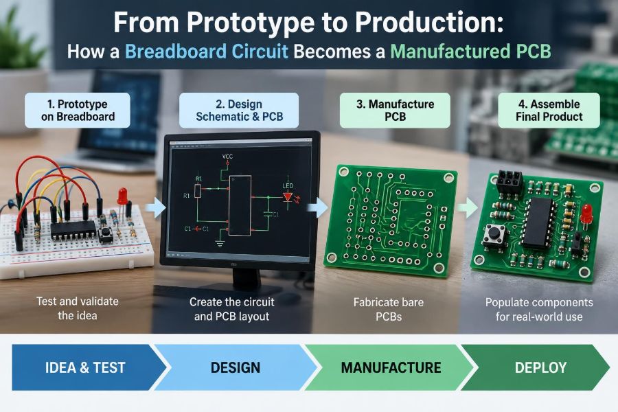

A circuit can look finished on a breadboard: an LED responds to a sensor, a microcontroller accepts a command, and the power supply reads the expected current. Then someone asks the question that changes the project: “Can we build fifty of these?”
At that point, the loose jumper wires and plug-in components that made experimentation so fast become a liability. The circuit must survive handling, fit into an enclosure, behave predictably, and be assembled more than once without relying on one person’s memory.
Moving from a breadboard to a manufactured printed circuit board, or PCB, is not simply a drawing exercise. It is a process of turning an electrical idea into a physical product with defined connections, component choices, manufacturing rules, test access, and documentation.
Understanding that process helps students make better prototypes and helps working engineers avoid a costly surprise: a circuit that works once on a bench but cannot be built, tested, or supported reliably.
🧭 The Shift From Experiment to Product
A breadboard is optimized for change. A PCB is optimized for repeatability. Those goals overlap, but they are not identical.
On a breadboard, moving a resistor takes seconds. On a PCB, changing that resistor may require editing the design files, ordering another fabrication run, and possibly revising assembly instructions. The production mindset therefore asks earlier questions: What is fixed? What can vary? What conditions must the circuit tolerate?
The objective is not to eliminate iteration. It is to make each iteration deliberate, documented, and easier to reproduce.
🧱 What a Breadboard Really Represents
A solderless breadboard is an electrical prototyping platform, not a miniature PCB. Its holes are connected in rows by spring contacts, while long side rails commonly distribute power.
Those hidden connections are convenient, but they can also mislead a designer. Different breadboard models arrange power rails differently, and split rails are a frequent source of mysterious “dead” circuits.
Breadboards also add resistance, capacitance, and inductance. At low speed these effects may be harmless; at higher frequencies or with fast digital edges, they can alter signals enough to hide problems or create new ones.
🔍 Confirm the Circuit Before Capturing It
Do not treat a working breadboard as proof that the design is ready for layout. First confirm that it works across the conditions it is expected to encounter.
For a small sensor board, that may mean trying the intended supply range, checking startup behavior, testing expected sensor extremes, and observing what happens when a cable is connected or removed. For a motor controller, it may include load transients and thermal behavior.
A useful question is: what evidence would convince you that the circuit is not merely working by accident?
📝 Create a Clear Functional Specification
Before opening PCB design software, write a concise specification. It turns informal expectations into engineering decisions that can be checked later.
- What input voltage range is permitted?
- What outputs, loads, connectors, and communications interfaces are required?
- What size, mounting, and enclosure constraints apply?
- What environment matters: desk use, vibration, moisture, temperature, or electrical noise?
- How will the board be programmed, tested, and identified?
This document need not be long. Even a one-page specification prevents layout decisions from being driven only by what was convenient on the breadboard.
📐 Redraw the Circuit as a Schematic
A schematic is the circuit’s logical map. It shows which electrical nets connect, what each component is, and how signals flow. It should be readable without looking at the breadboard.
Redrawing from scratch is often better than tracing wires one by one. Group power circuitry, sensing circuitry, control logic, and connectors so that a reviewer can follow the design. Name important nets, such as VIN, 3V3, GND, or I2C_SCL, consistently.
The schematic becomes the source of truth. A wire color or a remembered breadboard position should never be the source of truth.
🧠 Translate Prototype Shortcuts Into Real Circuit Decisions
Breadboard prototypes often contain implicit choices: a USB cable supplies power, a jumper acts as a connector, or a component’s lead length happens to limit current slightly. Production designs must make those choices explicit.
For example, if a development board supplied regulated 3.3 V during prototyping, determine whether the final PCB needs its own regulator, protection circuitry, and input connector. If a pushbutton was held by hand, choose its pull-up or pull-down resistor deliberately.
Every function should have a defined component, value, connection, and purpose.
⚙️ Choose Components for Availability and Assembly
The component that fits a breadboard is not automatically the right production component. Through-hole parts are easy to handle and ideal for many educational, repairable, and low-volume designs. Surface-mount devices can reduce size and support efficient assembly, but may demand more capable soldering and inspection.
Selection also involves package size, voltage and power rating, tolerance, operating temperature, lead time, and second-source options. A component is not fully specified by “10 kΩ”; its package, tolerance, power rating, and preferred manufacturer part number may all matter.
Where practical, avoid designing around a single difficult-to-source part unless its capability is genuinely necessary.
📦 Understand Footprints and Physical Packages
A schematic symbol represents electrical function. A footprint represents the copper pads, holes, outlines, and assembly information needed to mount the physical component on the PCB.
A common and expensive error is pairing a correct symbol with an incorrect footprint. A connector may have the right number of pins but the wrong pitch. An integrated circuit may be ordered in a different package from the one used in the library.
Always compare the footprint against the component manufacturer’s mechanical drawing. Check pin numbering, pad dimensions, body orientation, and connector mating direction.
🔗 Use Library Parts Carefully
PCB software libraries accelerate design, but library parts are engineering data, not unquestionable facts. Community libraries and older in-house libraries can contain errors or assumptions that do not match the part being purchased.
Review critical parts yourself, especially connectors, power devices, fine-pitch packages, unusual switches, and modules. For each, compare the schematic pin mapping and footprint to the current datasheet.
A small verification checklist is far cheaper than discovering that a connector is mirrored after boards arrive.
🧮 Define the Board Stack-Up and Layer Count
A basic PCB commonly uses two copper layers separated by insulating laminate. Many modest microcontroller and sensor boards work well on two layers when placement and routing are thoughtful.
More layers can provide cleaner power distribution, more routing space, and continuous reference planes for sensitive or fast signals. They also add fabrication cost and may be unnecessary for a simple design.
The right choice depends on signal speed, current, density, electromagnetic compatibility needs, and manufacturing constraints—not on a rule that more layers are always more professional.
📏 Set the Mechanical Boundary First
The board outline is an electrical constraint as much as a mechanical one. Define its size, mounting holes, edge clearances, connector locations, display openings, and keep-out zones before routing becomes dense.
If the PCB fits an enclosure, import or accurately recreate the enclosure dimensions. A board can pass every electrical test and still fail its purpose if a USB connector cannot reach the case opening or a mounting hole overlaps a standoff.
Also consider assembly access: can screws be installed, can a cable plug in, and can a test probe reach the necessary point?
🧩 Place Connectors Around the User Experience
Connectors, buttons, indicators, and mounting features are usually placed first because people and enclosures interact with them. Their locations should follow cable paths and user access, not the shortest possible trace.
A useful example is a sensor board inside a housing: placing its connector on the wrong edge may force a cable to bend sharply or cross another component. Repositioning it early is easy; repositioning it after routing may disrupt half the board.
Mark pin 1 clearly for connectors and polarized parts. Orientation marks are simple features that reduce assembly and service errors.
🗺️ Place Components by Current Flow and Function
After mechanical parts, place components so the circuit’s physical arrangement supports its electrical behavior. Keep each functional block compact: regulator and its capacitors together, microcontroller and decoupling capacitors close, analog sensor circuitry away from noisy switching nodes.
Follow the path of high current. Input protection should sit near the power entry; a switching regulator’s input and output capacitors should be close to the regulator pins indicated in its guidance.
Good placement reduces routing complexity. It often solves problems that cannot be fixed elegantly by clever trace paths.
⚡ Build a Solid Ground Return Path
Current does not disappear after reaching a load; it returns to its source. The path it takes matters. A ground plane, usually a broad connected copper area, gives return currents a low-impedance route and helps reduce voltage differences across the board.
For digital signals, return current tends to follow near the signal trace when a continuous reference plane is available. Splitting that plane beneath a fast signal can force a longer return route and increase noise or emissions.
“Ground is ground” is an oversimplification. Treat ground as a network carrying real current, especially near motors, converters, and high-speed digital interfaces.
🔋 Size Power Paths for Real Current
Thin traces are not universal wires. Their resistance causes voltage drop and heating, and narrow necks can become failure points when carrying substantial current.
Estimate expected and fault current, then select trace widths, copper area, connectors, fuses, and switches accordingly. Manufacturer calculators and fabrication guidance can help, but their assumptions should match the board’s copper thickness and environment.
Keep high-current loops short. A motor supply trace should not share a narrow section of copper with a precision sensor ground return if the resulting voltage disturbance can affect measurements.
🧼 Add Decoupling Where It Works
Decoupling capacitors supply short bursts of current close to an integrated circuit and shunt some high-frequency noise away from the power rail. They are not decorative components placed somewhere near the chip.
Place the recommended small capacitor close to each relevant power pin, with short connections to power and ground. The exact values and combinations depend on the component and application, so the component datasheet is the primary guide.
Bulk capacitance near power entry or changing loads can also help with slower supply disturbances, but it does not replace local decoupling.
📡 Route Sensitive and Fast Signals Intentionally
Not every trace needs special treatment, but some do. Clock lines, high-speed serial links, switching-regulator nodes, crystal connections, analog inputs, and radio-frequency paths are more sensitive to geometry and nearby noise.
Keep analog signals away from switching nodes and high-current traces. Keep crystal traces short and follow the microcontroller manufacturer’s recommendations. For controlled-impedance interfaces, trace width, layer stack-up, and reference plane must be planned together rather than guessed.
When requirements are uncertain, identify the risky nets early and consult the relevant component documentation or an experienced reviewer.
🛡️ Design for ESD, Transients, and Misuse
External connections expose a PCB to events that a breadboard may never see: electrostatic discharge from a person touching a connector, cable-induced transients, reversed power, or an incorrect supply.
Protection can include fuses or resettable protection, reverse-polarity arrangements, transient suppression devices, series resistors, filtering, and dedicated interface protectors. The right scheme depends on the connector, energy source, and safety requirements.
Protection is a trade-off. Extra parts add cost, board area, voltage drop, or signal capacitance, but omitting them can make a product fragile in normal use.
🌡️ Check Heat Before It Becomes a Field Failure
Any component that drops voltage while carrying current, switches substantial power, or drives a load can generate heat. A linear regulator, for example, dissipates power roughly in proportion to the voltage it drops and the load current it supplies.
Use package thermal information as an estimate, then validate with measurement under realistic worst-case conditions. Copper connected to thermal pads can help spread heat, but only if the footprint and layout are designed to use it.
A circuit that is comfortable during a short bench test may become unreliable after operating inside a sealed enclosure.
✅ Run Electrical and Design Rule Checks
Before manufacturing, use the PCB software’s electrical rule check (ERC) and design rule check (DRC). ERC looks for logical schematic issues such as unconnected pins or incompatible power definitions. DRC checks physical layout constraints such as trace spacing, hole size, copper clearance, and silkscreen overlap.
Do not dismiss warnings automatically. Some are intentional and can be documented; others reveal a mistaken net label, missing connection, or footprint collision.
Checks are filters, not proof. A design can pass them while still containing a wrong resistor value or a connector placed on the wrong edge.
👀 Review the Board as Another Engineer Would
A structured review catches errors that are easy to miss after hours of close work. Review the schematic, layout, 3D model if available, and manufacturing outputs separately.
- Trace every connector pin from the connector to its destination.
- Verify polarity for diodes, electrolytic capacitors, LEDs, batteries, and integrated circuits.
- Check programming headers, debug access, and boot-mode straps.
- Inspect copper clearances around mounting holes and enclosure hardware.
- Compare every critical footprint to the actual orderable part.
An independent reviewer is particularly valuable because they do not carry the designer’s assumptions.
🏭 Prepare Fabrication Files
The fabricator needs a precise description of the bare board. This commonly includes Gerber artwork files for copper, solder mask, silkscreen, and board outline, plus drill data and fabrication notes.
Modern board houses may also accept more integrated manufacturing formats, but the core principle remains: provide unambiguous layer, drill, and outline information. Open the generated files in an independent viewer before release.
Look for missing layers, incorrect board outlines, mirrored text, exposed copper where it should be covered, and drill holes that do not align with pads.
🤖 Separate Fabrication From Assembly Data
Fabrication creates the bare PCB. Assembly places and solders components. These activities require different information.
| Output | Primary purpose | Typical contents |
|---|---|---|
| Fabrication package | Make the bare board | Copper layers, mask, silkscreen, outline, drills |
| Bill of materials (BOM) | Buy correct components | References, values, quantities, approved part numbers |
| Pick-and-place file | Position assembly machine parts | Reference designators, coordinates, rotation, board side |
| Assembly drawing | Guide human inspection or assembly | Component outlines, polarity, notes, reference labels |
For hand assembly, the BOM and clear assembly drawing may be enough. For contract or automated assembly, coordinate conventions, rotations, substitutions, and panel requirements must be communicated carefully.
🧾 Build a BOM That Can Actually Be Purchased
A useful BOM is more than a list of generic values. It identifies the intended component in a way that a buyer or assembler can interpret consistently.
Include reference designator, quantity, value or description, package, manufacturer part number, and any approved alternatives. Mark parts that must not be substituted, such as precision references, safety-rated components, or a connector that must mate with a specific cable.
Review availability shortly before ordering. Supply conditions change, and a practical alternate can prevent an otherwise complete build from being delayed.
🧪 Plan Testing Into the Layout
Testing is easiest when the board was designed to be tested. Add accessible test points for key rails, ground, programming signals, reset, and important analog or communications nodes where appropriate.
A production test does not need to duplicate every laboratory measurement. It should efficiently detect likely assembly defects and verify the functions that matter to the product. For example, a fixture might confirm input current, regulated voltage, firmware communication, and an output response.
Test pads, fiducials for assembly alignment, and readable board revision markings add little complexity early and substantial value later.
🔧 Assemble the First Boards Cautiously
The first assembled PCB is a validation unit, not just a finished product. Inspect it before applying power: check orientation, solder bridges, missing parts, wrong values, and connector alignment.
Bring power up with a current-limited supply when possible. Measure resistance between power and ground beforehand, then verify each power rail before installing or enabling expensive modules and loads.
Work in stages. Confirm the supply, then the processor, then programming, then interfaces and loads. This narrows fault finding dramatically.
🐛 Debug Methodically When the PCB Does Not Behave
A nonworking first board is common and does not automatically mean the concept failed. Separate the problem into categories: schematic error, footprint error, assembly defect, firmware issue, layout-related behavior, or incorrect test setup.
Start with observable facts: supply voltage, current draw, clock activity, reset level, programming connection, and continuity. Compare the board against the schematic and known-good prototype rather than changing several things at once.
Document the root cause and correction. A temporary bodge wire can validate a hypothesis, but the design revision should capture the permanent fix.
🔁 Treat Revisions as Controlled Engineering Changes
Every board revision should have a clear identifier and a record of what changed. Revision control avoids the dangerous situation where two nearly identical boards require different firmware, assembly steps, or troubleshooting assumptions.
Record the reason for each change, the affected files, the verification performed, and whether old inventory remains usable. This discipline matters as much for a student team as for a commercial product.
A revision is successful when it resolves a defined issue without quietly introducing a new incompatibility.
⚠️ Common Breadboard-to-PCB Mistakes
Several mistakes appear repeatedly because breadboards forgive them. Recognizing them early improves the odds of a usable first revision.
- Assuming breadboard wiring is a complete schematic.
- Using a footprint without checking the package drawing.
- Forgetting local decoupling capacitors or placing them far from power pins.
- Routing high current through narrow traces or shared sensitive returns.
- Omitting programming, debug, and test access.
- Ignoring connector orientation, enclosure geometry, or mounting hardware.
- Ordering boards before reviewing manufacturing outputs.
None of these are signs of incompetence. They are predictable gaps between an experiment and a manufactured object.
🎯 Match Process Rigor to Project Risk
A hobby indicator board and a board controlling high energy, medical-related equipment, or safety-critical machinery do not require the same process. Higher-risk applications may require formal standards, specialized review, traceability, isolation analysis, certification planning, and qualified testing.
This article describes general PCB development practice, not a substitute for application-specific safety or regulatory engineering. When mains voltage, batteries capable of high fault current, radio compliance, or human safety is involved, seek appropriate expertise and follow applicable requirements.
Even for low-risk work, adopting a few professional habits—review, documentation, inspection, and staged test—pays off.
🌱 Let Production Thinking Improve the Prototype
Production constraints can improve early experimentation rather than slow it down. Use labeled wires, preserve a current schematic, measure supply behavior, select likely final connectors early, and note every value change made at the bench.
For a prototype likely to become a PCB, choose modules and parts that reveal the final electrical needs instead of concealing them. A development board may be appropriate, but understand which functions it provides behind the scenes.
The best prototype is not merely one that demonstrates an idea. It is one that teaches what the final design must become.
🚀 The Core Principle: Design for Repeatable Reality
A manufactured PCB is the physical contract between circuit theory, component data, mechanical constraints, manufacturing capability, and real-world use. It succeeds when those pieces agree, not when the layout simply looks tidy.
The transition from breadboard to PCB is therefore a sequence of translations: wires become nets, component leads become footprints, power assumptions become ratings, bench observations become test requirements, and personal knowledge becomes documentation.
Build the board so that another person can manufacture, assemble, test, and understand it without needing the original breadboard on the bench.
That mindset turns a one-off circuit into an engineered system—one that is easier to reproduce, debug, improve, and trust over its working life. 🔌🛠️📋