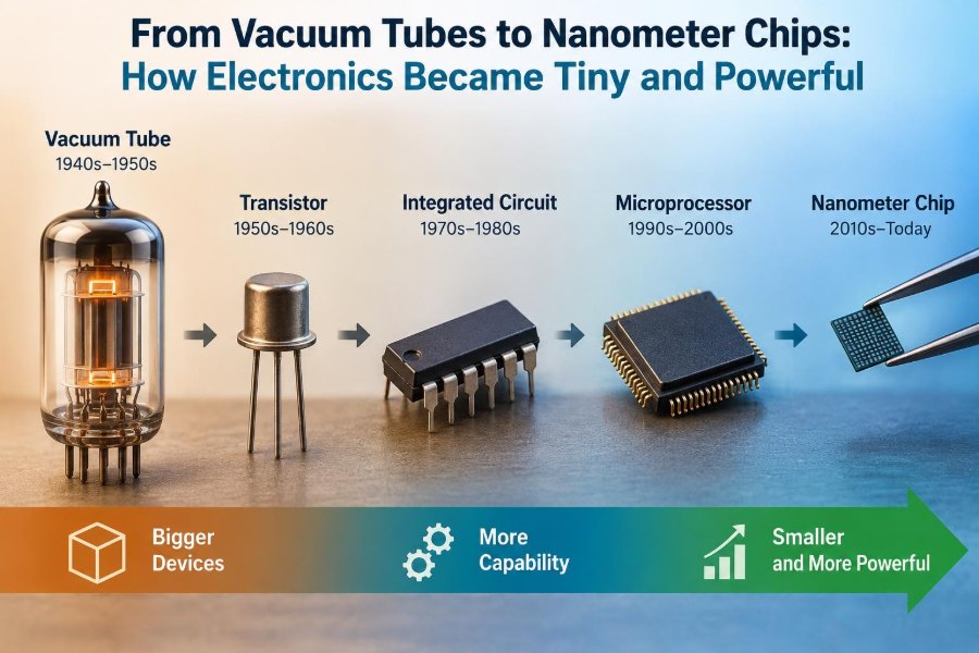

A smartphone can stream video, navigate a city, measure motion, and communicate across continents while fitting in a pocket. Its computing hardware contains billions of electronic devices, yet the first general-purpose electronic computers occupied rooms and demanded dedicated power and cooling.
That contrast is not merely a story of smaller parts. It is a story of new materials, new manufacturing methods, smarter circuit design, and difficult trade-offs involving heat, cost, reliability, and energy.
For electronics students, miniaturization explains why modern circuits look and behave so differently from early equipment. For working professionals, it remains a daily design constraint: a smaller product is useful only if it can still be manufactured, powered, tested, repaired, and trusted.
The path from glowing vacuum tubes to nanometer-scale chips shows a central lesson of engineering: making something smaller often changes what it is capable of doing.
📻 Electronics Before the Transistor
Early electronic systems used vacuum tubes: sealed glass or metal devices that controlled electron flow through a vacuum. Tubes could amplify weak signals, switch circuits, and generate radio-frequency signals, making them essential to radio, television, radar, and early digital computers.
A typical tube required a heated cathode to emit electrons. This heater consumed power and produced heat even before the circuit performed useful work. Tubes were also relatively large, fragile, and limited in operational life compared with later solid-state devices.
🔥 Why Vacuum-Tube Systems Were So Large
The tube itself was only part of the space problem. Equipment also needed sockets, wiring, transformers, resistors, capacitors, ventilation, and mechanical access for maintenance. Thousands of point-to-point wires made assembly labor-intensive and fault finding slow.
Large computers faced a practical reliability problem: if a system contains many components, even a modest failure rate per part produces frequent failures somewhere in the machine. Heat accelerated wear and made this challenge worse.
⚡ The Transistor Changes the Building Block
The invention of the transistor introduced a device that controlled current inside a semiconductor rather than through a vacuum. A semiconductor is a material, commonly silicon, whose electrical behavior can be carefully adjusted by adding small amounts of selected impurities.
Transistors could perform the switching and amplification roles of tubes while using far less power and occupying much less volume. They also avoided heater warm-up time and were generally more rugged, which made portable electronics realistic.
🧱 Semiconductor Materials Make Control Possible
Silicon becomes useful because its conductivity can be engineered through doping. Adding donor atoms creates n-type material with extra mobile electrons; adding acceptor atoms creates p-type material with mobile holes, which behave as positive charge carriers.
When p-type and n-type regions meet, they form a p-n junction. This junction can control current direction and response to voltage. Diodes, bipolar transistors, and field-effect transistors all rely on deliberately shaped semiconductor regions.
🪄 From Individual Parts to Integrated Circuits
Early transistorized products still connected separate transistors, resistors, capacitors, and diodes on circuit boards. That improved size and reliability, but each connection remained a possible defect, parasitic element, or assembly cost.
An integrated circuit, or IC, fabricates many devices and their interconnections on one piece of semiconductor material. This removed a huge amount of manual wiring and enabled functions that would have been impractical with discrete components.
🧪 The Planar Process Enables Mass Production
IC manufacturing became scalable through the planar process, in which layers are formed across a flat silicon wafer. Oxide layers can protect surfaces or act as electrical insulation, while openings allow selected regions to be modified.
The key insight was repeatability. Instead of assembling each transistor individually, manufacturers could process hundreds or thousands of identical dies across one wafer using controlled chemical, thermal, and optical steps.
📷 Photolithography Draws Circuits with Light
Photolithography transfers patterns onto a wafer using light-sensitive material called photoresist. A mask or reticle defines where light reaches the resist; development then reveals a pattern that guides later processing.
The pattern may define transistor gates, implanted regions, contacts, or metal wires. Modern lithography is far more sophisticated than simple photography, but the basic idea remains recognizable: use precisely controlled light to reproduce extremely small features.
🧼 Cleanrooms Protect Tiny Features
As features shrink, ordinary dust becomes enormous by comparison. A particle can block a pattern, bridge a conductor, or damage a transistor region. Semiconductor fabrication therefore occurs in cleanrooms with filtered air, specialized clothing, and tightly controlled processes.
Cleanliness is not cosmetic. Yield—the fraction of manufactured dies that meet specification—depends strongly on defect control. A sophisticated design has little commercial value if too few working chips emerge from the fabrication line.
📐 What “Nanometer” Really Means
A nanometer is one billionth of a meter. In chip discussions, a process-node label expressed in nanometers is no longer a simple measurement of one physical dimension. It is mainly a technology-generation name.
That distinction matters. Comparing nodes by name alone can be misleading across manufacturers. Useful comparisons also consider transistor density, performance, power behavior, available design rules, and manufacturing maturity.
🚦 MOSFETs Become the Dominant Switch
Most digital chips are built primarily from MOSFETs, metal-oxide-semiconductor field-effect transistors. A voltage at the gate controls whether a conductive channel forms between source and drain terminals.
The gate is electrically insulated from the channel by a thin dielectric. Because the gate ideally draws very little steady-state current, MOSFET-based logic can be highly energy-efficient, especially when it is not switching.
🔁 CMOS Makes Digital Logic Efficient
Complementary MOS, or CMOS, pairs n-channel and p-channel transistors. In a basic CMOS inverter, one transistor connects the output toward the supply while the other connects it toward ground.
In a stable logic state, ideally one path is off, so there is little direct current from supply to ground. Real chips still consume leakage power, and switching consumes energy, but CMOS dramatically improved the viability of dense digital systems.
📉 Scaling Shrinks Both Devices and Delays
Smaller transistors can reduce the distance signals travel and lower the capacitance that must be charged and discharged. In favorable conditions, this supports faster switching and allows more devices in a given area.
Scaling also brought economic leverage: a wafer can contain more dies when each die is smaller. But this benefit is conditional. Advanced fabrication equipment, masks, verification, and yield challenges can make newer nodes extraordinarily expensive.
🔋 Why Switching Costs Energy
A digital gate consumes dynamic energy when it charges or discharges capacitance. A useful approximation is that switching energy rises with capacitance and with the square of supply voltage. This is why voltage reduction has been so valuable.
Frequency matters too: switching a circuit more often raises power demand. The familiar engineering tension follows directly—higher clock rates can improve throughput, but they also make power delivery and cooling harder.
🌡️ Heat Becomes the Modern Constraint
Power that is not delivered to useful external work ultimately becomes heat. In a compact chip, heat must travel through silicon, packaging materials, a heat spreader, and often a heatsink before reaching surrounding air or a cooling loop.
Excess temperature can reduce performance, worsen leakage, shorten component life, and create mechanical stress. This is why a thin laptop may slow down during sustained workloads even though it feels powerful at first.
🕳️ Leakage Complicates Tiny Transistors
As transistor dimensions and insulating layers became extremely small, unwanted current paths became harder to suppress. Leakage current is current that flows when a device is intended to be off or when stored charge should remain in place.
Leakage is especially relevant for battery-powered devices and dense processors. Designers address it with improved transistor structures, power-gating techniques, multiple threshold-voltage options, and careful control of operating conditions.
🏗️ Three-Dimensional Transistor Structures
Traditional planar transistors place the channel near the surface of the wafer. At small dimensions, controlling that channel from only one side becomes difficult. FinFETs improved control by wrapping the gate around a raised, fin-like channel.
Newer gate-all-around approaches surround the channel more completely. These structures are not magic solutions, but stronger electrostatic control can help reduce leakage and support continued scaling.
🧩 Interconnects Can Matter More Than Transistors
A chip is not just a collection of switches. It is also a vast network of metal wires that distribute power, clocks, and data. As devices become smaller, wire resistance, capacitance, congestion, and signal delay become major design limitations.
Engineers use multiple metal layers, different wire widths, buffering, shielding, and careful floorplanning. A fast transistor does not guarantee a fast system if the signal spends too long traveling through interconnect.
🧠 Architecture Multiplies the Value of Silicon
Miniaturization provided more transistors, but chip architects had to decide how to use them. Designers added caches, pipelines, multiple cores, specialized accelerators, larger memories, and sophisticated power-management circuits.
A graphics processor, digital signal processor, or machine-learning accelerator can perform a narrow class of operations more efficiently than a general-purpose CPU. The gain comes from matching hardware organization to the workload, not from transistor count alone.
💾 Memory Follows a Different Set of Trade-Offs
Logic transistors emphasize switching behavior, while memories emphasize how bits are stored, accessed, and retained. SRAM is fast and commonly used for processor caches, but it uses multiple transistors per bit. DRAM stores charge in tiny capacitors and needs periodic refresh.
Nonvolatile memories retain information without power, but they bring different endurance, speed, and write-energy characteristics. There is no universally best memory; systems combine types to balance capacity, speed, power, and cost.
📦 Packaging Is Part of the Electronic System
A die cannot simply be exposed silicon. Packaging protects it, delivers power, carries signals to the circuit board, and helps remove heat. At high speed, the package also affects electrical performance through inductance, resistance, and signal integrity.
Modern packages may place several dies close together, stack them, or connect them with dense short links. This approach can improve bandwidth and combine technologies that are not economical or practical to fabricate on one monolithic die.
🧱 Chiplets Offer Another Route to Progress
A chiplet is a smaller functional die designed to work with other dies in one package. For example, compute, input/output, cache, and specialized processing functions may be separated rather than built as one giant chip.
Chiplets can improve yield because defects ruin a smaller die rather than an entire very large die. They also introduce challenges: fast die-to-die links, package design, thermal coupling, testing, and standards for interoperability all matter.
🛠️ Design Automation Handles Unmanageable Complexity
A modern chip may contain far too many devices and connections for a team to place manually. Electronic design automation tools translate logical descriptions into physical layouts while checking timing, power, manufacturability, and rule compliance.
Automation does not remove engineering judgment. Constraints, libraries, clocking strategy, verification plans, and architectural choices must be correct. A tool can optimize within its instructions; it cannot rescue an unclear specification.
✅ Verification Prevents Expensive Mistakes
Fabricating a chip is slow and costly, so discovering a design error after production can be serious. Verification compares intended behavior with implemented behavior through simulation, formal methods, emulation, and many specialized checks.
Physical verification checks whether layout obeys manufacturing rules. Timing analysis checks whether signals arrive when required. Power analysis examines voltage drop and current-related risks. Each discipline addresses a different failure mode.
🔌 Power Delivery Is More Than a Battery Question
Every transistor switch draws current from a power network. If many circuits switch together, local voltage can dip because package and interconnect resistance and inductance oppose sudden current change. This is often called supply noise or voltage droop.
Designers use decoupling capacitors, robust power grids, multiple voltage domains, and controlled activity. For board designers, the same principle applies: power integrity must be planned alongside signal routing, not added at the end.
📡 Analog Electronics Did Not Disappear
Digital logic dominates computation, but physical signals are usually analog. Microphones, antennas, sensors, power converters, and radio circuits handle continuous voltages, currents, frequencies, and noise.
Analog design does not always benefit from aggressive scaling in the same way as digital logic. Precision, voltage headroom, matching, passive components, and noise can favor specialized processes or mixed-signal integration rather than the smallest available node.
🧰 Practical Lessons for Circuit Designers
When choosing components or designing a board, do not equate a smaller package with a better design. Small parts can reduce parasitics and board area, but they may be harder to inspect, rework, cool, or hand-assemble.
- Read the datasheet for voltage limits, thermal data, recommended layout, and decoupling guidance.
- Keep high-current loops short and provide clear return paths for fast signals.
- Use adequate test points and consider how the product will be diagnosed after assembly.
- Choose a package and process that match production capability, not just a schematic ideal.
⚠️ Common Misunderstandings About Miniaturization
One common mistake is assuming that a smaller process node automatically means a faster final product. Software, memory bandwidth, thermal limits, architecture, and power settings may dominate real-world performance.
Another is treating more transistors as inherently better. Unused hardware still occupies area and may add leakage or design complexity. Effective engineering is about meeting a requirement with an acceptable balance of performance, energy, cost, reliability, and time.
♻️ Repairability and Electronic Waste
Highly integrated products can be reliable and compact, but integration may make repair more difficult. A failed function that once involved a replaceable discrete component may now be inside a fine-pitch package or a single system-on-chip.
Designers can improve serviceability through documentation, diagnostics, replaceable modules where appropriate, durable connectors, and realistic thermal margins. These choices may increase size or cost, so they must be evaluated against the product’s intended life and use.
🌍 The Supply Chain Behind a Tiny Chip
A chip embodies far more than the final silicon die. It depends on ultra-pure materials, specialized chemicals, fabrication equipment, design software, advanced packaging, test equipment, and global logistics.
This complexity explains why electronics development involves supply risk and long lead times. A technically suitable part may not be a practical choice if it cannot be sourced consistently, tested appropriately, or supported over the product lifecycle.
🔭 Beyond Simple Shrinking
Future progress will not rely on one path alone. Better transistors, advanced packaging, heterogeneous integration, new memory approaches, improved power conversion, optical links in selected applications, and more efficient algorithms can all contribute.
Some technologies will target maximum compute density; others will prioritize low energy, radiation tolerance, long operating life, high voltage, or easy manufacturability. Electronics advances through diverse solutions because applications have diverse constraints.
🎓 The Core Principle: Integration Creates Capability
The journey from vacuum tubes to nanometer chips is best understood as a chain of reinforcing improvements. Smaller and more reliable switches enabled dense circuits; dense circuits enabled complex architectures; better manufacturing and packaging made those architectures practical.
The central lesson is not that every device should be made as small as possible. Miniaturization is valuable when it improves the complete system: function, energy use, reliability, cost, manufacturability, and human usefulness.
Electronics became tiny and powerful because engineers learned to control matter, charge, heat, and information together—not because size alone solved the problem. That systems view remains the most useful guide for the next generation of devices. 🔌🧠🌱