
A new laptop may look almost identical to last year’s model, yet it can run larger AI models, edit video more smoothly, or deliver longer battery life. Those gains are not always coming from transistors that are dramatically smaller than before.
For decades, the usual picture of semiconductor progress was simple: shrink the transistors, fit more of them onto one silicon die, and get faster, cheaper electronics. That approach remains valuable, but it has become harder, more expensive, and less universally effective.
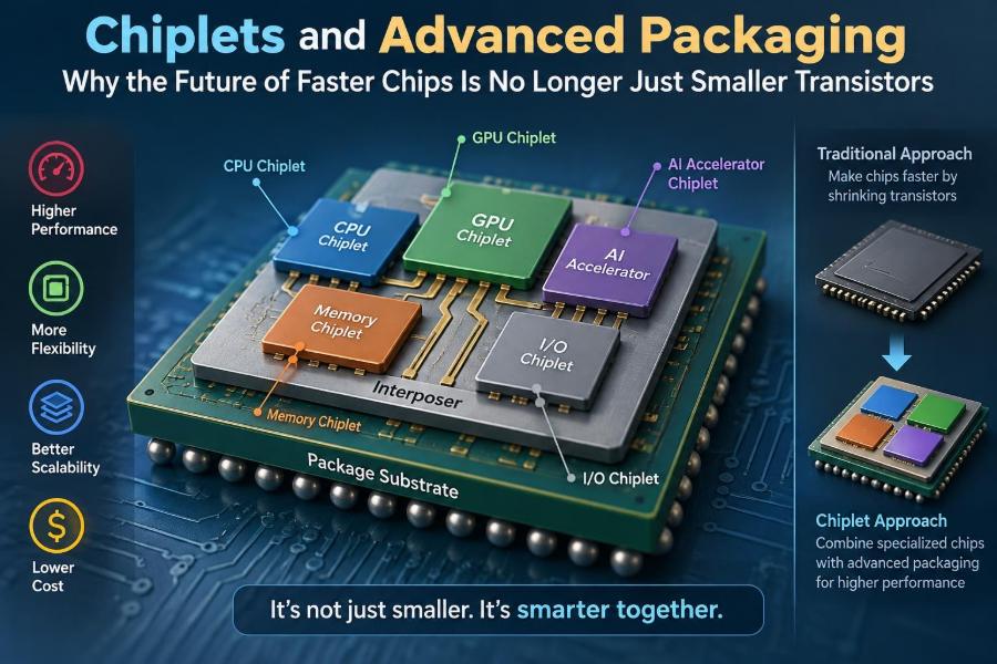
Meanwhile, a modern processor increasingly resembles a carefully organized neighborhood rather than a single giant building. Compute blocks, memory, input/output circuitry, and specialized accelerators may be built separately and then connected inside one package.
This shift toward chiplets and advanced packaging is changing what engineers mean by a “chip.” It affects performance, power, manufacturing yield, testing, architecture, and even the skills needed to design electronic systems.
🧩 The old model: one large monolithic die
A conventional integrated circuit is monolithic: most or all functions are fabricated on one continuous piece of silicon, called a die. A CPU, cache memory, graphics logic, and interfaces may share that die.
This arrangement has obvious strengths. Signals can travel over very short on-chip wires, designers can tightly optimize the full layout, and manufacturing flow is comparatively direct once the design is mature.
But making one very large, leading-edge die creates a difficult dependency: every major function must be ready for the same process technology, manufacturing schedule, and design revision.
📉 Why transistor scaling is getting harder
Transistor scaling still provides gains, but those gains no longer arrive with the predictability associated with earlier generations. At extremely small dimensions, controlling leakage, variation, heat, and manufacturing defects becomes more challenging.
New process nodes also demand more complex patterning, sophisticated device structures, and tighter process control. The resulting development and fabrication costs are high enough that only products with sufficient volume or value can justify the newest node.
Crucially, a smaller transistor does not automatically make every part of a system better. Analog circuits, high-voltage interfaces, radio-frequency blocks, and large I/O structures may gain little from being moved to the most advanced logic process.
💰 The economic problem with giant dies
A silicon wafer contains a finite area. When a die becomes larger, fewer dies fit on that wafer, and each die has more area in which a manufacturing defect can occur.
This affects yield, the fraction of fabricated dies that pass required tests. A small defect may disable a large monolithic processor, even if most of its transistors function correctly.
Yield depends on many factors, including defect density, design rules, redundancy, and test strategy. Still, the general engineering principle is clear: dividing a very large design into smaller pieces can reduce the amount of valuable silicon lost when defects occur.
🧱 What a chiplet actually is
A chiplet is a relatively small die designed to provide a defined function within a larger package-level system. It might contain CPU cores, graphics hardware, a memory cache, a network switch, I/O controllers, or an AI accelerator.
Chiplets are not simply “small chips placed near each other.” Their value depends on high-bandwidth, low-energy connections and on an architecture that treats the package as a coordinated system.
A chiplet-based product can combine several copies of one compute tile with other specialized dies. This lets the designer scale performance by adding tiles rather than redesigning one enormous processor.
📦 A package is now part of the system
Historically, the package primarily protected a die and connected it to the circuit board. In advanced packaging, the package becomes an active electrical and mechanical structure that provides dense interconnect, power delivery, heat removal, and sometimes memory integration.
This is often described as heterogeneous integration: combining components that may use different process technologies, materials, or functions into one closely coupled assembly.
The distinction matters because data movement consumes energy and time. Moving data across a motherboard is very different from moving it across a short, wide connection inside a package.
🛣️ Interconnect is the central engineering challenge
Dividing a large die creates boundaries, and every boundary needs an interconnect. If those links are too slow, too power-hungry, or too costly, chiplets lose much of their advantage.
Package-level links usually use many parallel connections operating over short distances, rather than relying only on a few very fast long-reach serial lanes. A wide interface can move substantial data while avoiding some of the power overhead associated with long off-package channels.
Latency also matters. A processor core waiting for data from a neighboring chiplet may experience delays that affect software performance, especially for fine-grained communication.
🔌 Die-to-die links versus board-level links
Board-level interfaces must drive signals through package balls, printed-circuit-board traces, connectors, and a comparatively noisy electrical environment. They need robust signaling, equalization, and often substantial energy per transmitted bit.
Die-to-die links travel much shorter distances and can use much finer-pitch connections. That can support higher connection density and lower energy, although the exact benefit depends on the package technology and signaling scheme.
Designers must not assume every chiplet connection behaves like an on-die wire. It remains a real interface with protocol overhead, clocking requirements, test needs, and failure modes.
🔗 Standards can make chiplets more reusable
A proprietary chiplet interface can be highly optimized for one company’s products, but it may limit interoperability. Open or widely adopted die-to-die interface approaches aim to make it easier for compatible chiplets to communicate within a package.
Standardization does not mean all chiplets will become interchangeable commodities. Electrical requirements, physical dimensions, security expectations, thermal limits, and software integration still vary widely.
Its practical value is reducing unnecessary reinvention. A defined interface gives designers a clearer boundary between the logic inside a chiplet and the transport mechanism connecting it to others.
🏗️ 2D packaging and organic substrates
Many multi-die packages place chiplets side by side on an organic substrate. The substrate routes signals between dies and connects the package to the system board.
This approach can be more practical than a single huge die and is well suited to modular designs. However, routing density is limited compared with silicon-based interconnect structures, and the physical separation between dies can be greater.
For applications with moderate bandwidth demands, this may be an excellent compromise between capability, cost, and manufacturability.
🪜 2.5D integration with an interposer
In 2.5D packaging, multiple dies sit side by side on a fine-pitch interposer, commonly made from silicon or another high-density routing material. The interposer provides many short connections between dies.
This is particularly useful when logic must communicate intensively with high-bandwidth memory. Instead of forcing memory traffic through longer board-level paths, the memory stacks can sit close to the processing die or chiplets.
The term “2.5D” reflects the geometry: components are primarily arranged laterally, but the integration density is far beyond ordinary board assembly.
🏢 3D stacking brings functions closer
3D integration stacks dies vertically. Vertical connections can be formed using technologies such as through-silicon vias, which are conductive paths passing through silicon, or very fine direct bonding connections between die surfaces.
Stacking shortens some signal paths dramatically and can increase bandwidth per unit area. It is attractive for memory-on-logic arrangements, cache stacking, and compact high-performance systems.
But vertical integration also concentrates heat and complicates test, repair, and mechanical assembly. A design that looks ideal electrically may become difficult to cool in a real product.
🧠 Memory bandwidth is a major driver
Many modern workloads are limited less by arithmetic capability than by how quickly data reaches the compute engines. AI inference, graphics, scientific simulation, and large database operations can all demand enormous memory bandwidth.
Advanced packages can place wide memory interfaces close to compute logic. This reduces the distance and pin limitations that make conventional external memory interfaces difficult to scale indefinitely.
High-bandwidth memory is not a universal solution. It can raise package complexity and cost, so systems with modest bandwidth needs may be better served by conventional memory arrangements.
⚡ Data movement often dominates energy use
Performing a simple arithmetic operation can require less energy than fetching the necessary data from distant memory. This is why architecture increasingly focuses on locality: keep frequently used data physically close to the logic that consumes it.
Chiplets enable specialized memory hierarchies, shared caches, and near-memory compute structures. They do not eliminate data movement, but they give designers additional physical options for reducing it.
For embedded engineers, the lesson applies even outside advanced processors: reducing unnecessary data transfers can improve power consumption as effectively as optimizing the arithmetic itself.
🧪 Mixing process technologies intelligently
One of the strongest arguments for heterogeneous integration is process specialization. A compute chiplet may use an advanced logic node, while I/O, analog, power-management, or security functions use a process selected for voltage tolerance, analog behavior, nonvolatile memory, or cost.
This avoids using expensive leading-edge silicon where it provides little system benefit. It can also allow proven interface circuitry to remain on a stable process while compute logic evolves more quickly.
Integration is not effortless, however. Different dies may have different voltage domains, thermal expansion behavior, design rules, and reliability characteristics.
🎯 Specialization changes processor architecture
General-purpose CPUs remain essential, but many workloads benefit from dedicated hardware. A system may pair CPU chiplets with graphics tiles, neural-processing engines, media encoders, encryption blocks, or network accelerators.
Specialization can improve performance per watt because the hardware is shaped around a narrower task. The trade-off is reduced flexibility and the additional work needed to schedule data and software correctly.
A useful analogy is a workshop. One versatile tool can complete many jobs, but dedicated tools often perform recurring tasks faster, with less waste, once the workflow justifies them.
🧮 Scaling by replication
Chiplets make replication a practical architecture strategy. Rather than designing one larger compute die, a manufacturer can use several instances of a validated compute tile and connect them through a fabric.
This supports product families. A lower-tier product may use fewer compute chiplets, while a higher-tier version uses more of the same tiles plus greater memory capacity or I/O capability.
Software and interconnect topology determine whether replication scales efficiently. If every chiplet constantly accesses remote data, traffic congestion and latency can erode the expected gain.
🧭 The fabric determines system behavior
The fabric is the communication network linking chiplets, memory controllers, and I/O blocks. It carries requests, data, coherence messages, and control traffic.
Design choices include topology, routing policy, bandwidth allocation, and whether caches remain coherent across chiplets. Cache coherence means different processing elements can maintain a consistent view of shared memory, but enforcing it can generate significant traffic.
A good fabric is not merely fast at peak throughput. It must behave predictably under congestion, isolate faults where possible, and provide enough observability for validation and debugging.
🌡️ Thermal design becomes a package problem
Heat has always limited high-performance electronics, but dense multi-die assemblies make thermal planning more interdependent. A hot compute die can warm nearby memory or I/O dies, reducing their margin even when those dies consume less power themselves.
Stacked arrangements are especially demanding because an upper die may sit farther from the heat spreader. Thermal paths, die placement, power maps, cooling hardware, and workload scheduling must be considered together.
Engineers use simulation and measurement to identify hot spots, but real workloads matter. A package may pass a simple power test while still showing local thermal stress during sustained accelerator use.
🔋 Power delivery must cross more boundaries
Every chiplet needs stable power across changing loads. Package routing, bumps, inductance, decoupling capacitors, and voltage-regulator behavior all influence voltage droop and noise.
Fine-pitch die connections provide more paths, yet dense packages also make power-integrity analysis harder. Switching activity in one die can affect supply behavior in another through shared package and board structures.
Power delivery is therefore not a final layout detail. It is an architectural constraint that can influence chiplet placement, clock targets, interface activity, and permissible workload combinations.
🧷 Mechanical stress and reliability matter
Silicon, substrates, solder structures, and molding materials expand differently as temperature changes. Repeated thermal cycling can create mechanical stress in interconnects and package structures.
Advanced packages also introduce many assembly steps: attaching dies, forming micro-bumps or bonded interfaces, adding memory stacks, encapsulating, and testing. Each interface adds opportunities for defects or long-term reliability concerns.
Reliability qualification must reflect actual use conditions. A data-center accelerator, automotive controller, and consumer phone may face very different temperature ranges, duty cycles, vibration environments, and service-life expectations.
🔍 Testing is harder than testing one die
A known-good die is a die that has passed tests before package assembly. Using known-good dies is desirable because assembling several expensive dies and discovering one failure afterward is costly.
Yet pre-package testing cannot catch every issue. Some faults emerge only when dies communicate at full speed, share power supplies, or operate at package-level temperatures.
Test access is also constrained after stacking. Designers may need built-in self-test, loopback paths, boundary scan features, repair mechanisms, and telemetry designed in from the beginning.
🛡️ Security boundaries can shift inside the package
More dies and more interfaces expand the system’s attack surface. A secure design must consider authentication, key storage, debug access, firmware loading, side-channel behavior, and trusted communication between chiplets.
Chiplets sourced from different design teams or supply chains may require clear trust assumptions. A physical proximity advantage does not automatically make an interface secure.
Security architecture should define which components are trusted, how they prove identity, and what happens when communication fails or behaves unexpectedly. Retrofitting these decisions late is difficult.
🧰 Software still sees the consequences
Packaging is physical, but software experiences its effects through memory latency, bandwidth, accelerator availability, and topology. Operating systems, drivers, compilers, and runtime libraries may need to understand where compute and memory resources reside.
For example, scheduling a task near the memory it uses can reduce remote traffic. Applications that divide work into well-localized chunks often use multi-chiplet hardware more effectively than applications with constant global sharing.
Hardware alone cannot guarantee a speedup. Performance depends on the workload, algorithm, data layout, and quality of the full software stack.
📊 When chiplets beat monolithic integration
Chiplets are particularly compelling when a design needs very large compute area, expensive leading-edge logic, substantial memory bandwidth, or a mix of functions that benefit from different manufacturing processes.
They can also improve reuse across a product line. Reusing a mature compute or I/O tile can shorten development risk compared with redesigning every block for every new product.
| Design situation | Monolithic die may suit | Chiplet approach may suit |
|---|---|---|
| Compact, modest-complexity controller | Low interface overhead and simpler assembly | Usually unnecessary unless reuse is unusually valuable |
| Large high-performance processor | Useful if yield and die size remain manageable | Scalable compute tiles and improved yield economics |
| Mixed analog, I/O, and advanced logic | One process may force compromises | Each function can use a more suitable process |
| Bandwidth-hungry accelerator | External memory connections can constrain scaling | Dense package links to nearby memory are attractive |
🚫 When chiplets are the wrong answer
A chiplet partition adds interfaces, packaging cost, validation work, and thermal complexity. For a small microcontroller or a cost-sensitive consumer IC, a single die may remain the simpler and better solution.
Chiplets can also be unsuitable when a function requires exceptionally tight timing across a broad area or when package-level latency would disrupt the design. Partitioning must be justified by measurable system advantages.
The right question is not “Can this become chiplets?” but “Does the total product benefit exceed the extra integration burden?”
⚠️ Common misconceptions to avoid
- “Chiplets always cost less.” Smaller dies can improve yield, but advanced assembly, substrates, interposers, and test may be expensive.
- “Packaging is just manufacturing.” Package interconnect and thermal behavior directly shape architecture and performance.
- “More chiplets always mean more speed.” Communication, coherence, and memory bottlenecks can limit scaling.
- “3D stacking is automatically superior.” It can provide extraordinary density, but cooling and test constraints are substantial.
- “A standard interface solves integration.” Protocol compatibility is only one part of electrical, mechanical, thermal, and security co-design.
🧑💻 Skills electronics engineers need
Advanced packaging rewards engineers who can work across traditional boundaries. Digital designers need awareness of physical interconnect limits; package engineers need visibility into traffic patterns and power maps; system engineers need to understand process and yield trade-offs.
Useful areas to develop include signal integrity, power integrity, thermal analysis, high-speed interfaces, testability, hardware security, and performance modeling. Familiarity with floorplanning is increasingly valuable because physical placement affects system behavior.
Students can begin with smaller exercises: compare a narrow fast serial link with a wide parallel interface, model memory bottlenecks, or examine how package parasitics affect a power rail.
🔬 A practical way to evaluate a partition
Before dividing a design into chiplets, identify the data flows. Which blocks exchange the most data? Which functions need the newest process node? Which blocks change frequently, and which can be reused for years?
- Estimate bandwidth, latency, and energy requirements between candidate partitions.
- Map power density and cooling paths before choosing a stack or side-by-side layout.
- Compare full cost, including test, assembly, substrate, yield, and qualification.
- Define debug, repair, security, and production-test access early.
- Validate with realistic workload traces rather than peak-throughput assumptions alone.
This process turns chiplets from a fashionable label into an engineering decision grounded in constraints.
🌍 Effects beyond high-end processors
The most visible examples may be data-center processors and AI accelerators, but the underlying methods can influence networking equipment, industrial systems, automotive electronics, communications hardware, and specialized embedded platforms.
Adoption will vary. High-volume or high-performance products can absorb sophisticated packaging sooner, while simpler products may continue to rely on conventional packages for a long time.
The broader effect is a widening design space: engineers can optimize at the transistor level, die level, package level, board level, and software level simultaneously.
🔮 The future is co-design, not a single miracle
No single packaging method will replace all others. Monolithic dies, 2D multi-die packages, interposer-based systems, and 3D stacks will coexist because they solve different combinations of cost, bandwidth, power, density, and reliability requirements.
The most successful future designs will be co-designed across disciplines. Device technology, circuit design, architecture, packaging, cooling, firmware, and applications must be considered as connected parts of one system.
That is the deeper change: semiconductor progress is becoming less about one dimension of a transistor and more about the quality of the connections around it.
✅ The core takeaway: performance now crosses the die boundary
Smaller transistors remain foundational, but they are no longer the only practical route to better chips. Chiplets allow a system to scale, reuse proven building blocks, mix process technologies, and place memory or accelerators closer to where they are needed.
Those advantages come with real costs: more demanding interconnect design, package-level power and thermal challenges, complex testing, and tighter hardware-software coordination. The best implementation depends on the product rather than on a universal packaging trend.
For engineers, the key mental shift is to treat the package as part of the architecture. Once the die boundary becomes a design variable, new ways of improving performance, efficiency, and manufacturability become possible.
The future of faster chips will be defined not only by smaller transistors, but by smarter ways of assembling, connecting, powering, cooling, and programming silicon. 🔬🧩⚡