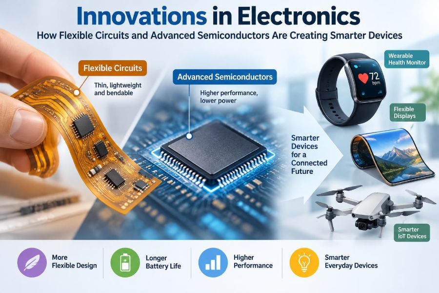

A fitness band tracks a pulse while its strap bends around a wrist. A phone camera brightens a dim room in a fraction of a second. A car notices an object near its bumper and warns the driver. These experiences feel simple because the electronics inside them are doing the complicated work quietly.
Two technology shifts make much of that work possible: circuits that can conform to curved or moving surfaces, and semiconductor devices that compute, sense, communicate, and manage power with far greater efficiency than earlier generations.
Neither development replaces the other. Flexible circuits provide a practical physical path for signals and power in constrained spaces, while advanced semiconductors provide the intelligence and conversion efficiency that make a device responsive rather than merely electronic.
For students and practicing engineers, the useful question is not whether a product is “smart.” It is how mechanical design, materials, packaging, signal integrity, software, and power limits combine to make smart behavior reliable in the real world.
🧭 The Meaning of a Smarter Device
A smarter device senses conditions, processes information, makes a decision, and produces a useful response. A thermostat, for example, measures temperature, runs a control algorithm, and switches heating or cooling equipment.
That definition includes far more than artificial intelligence. Smart behavior can come from a simple microcontroller, a specialized sensor interface, or a powerful processor running local machine-learning inference.
🧩 The Electronics Stack Behind Everyday Products
Most connected products contain several layers of function: sensors acquire physical data, analog circuits condition weak signals, processors make decisions, radios exchange information, and power circuits keep every block operating safely.
Flexible interconnects and semiconductors sit across this stack. One helps arrange the system physically; the other performs its electrical functions.
📜 What a Flexible Circuit Actually Is
A flexible printed circuit, often called an FPC or flex circuit, is a patterned conductive circuit built on a bendable insulating film rather than a rigid fiberglass-reinforced board. Copper traces carry signals and power, while polymer layers provide insulation and protection.
It is not simply a rigid PCB that happens to bend once. A well-designed flex circuit is engineered around bend radius, material strain, conductor geometry, and expected motion.
🧵 Common Materials in Flex Construction
Polyimide is widely used because it tolerates elevated processing and operating temperatures while remaining flexible. Adhesiveless copper-clad laminates, coverlays, stiffeners, and carefully selected adhesives are also common parts of a finished construction.
Material choice affects more than flexibility. It influences dimensional stability, moisture behavior, impedance control, assembly temperature tolerance, and long-term durability.
🔄 Static Flex, Dynamic Flex, and Rigid-Flex
A static flex bends during installation but then stays in place, such as the cable joining a display to a main board. A dynamic flex bends repeatedly during operation, as in a printer head or a hinged mechanism.
Rigid-flex boards combine rigid PCB sections with flexible sections in one integrated assembly. They can remove connectors and cables, but their fabrication rules and repair considerations are more demanding.
| Construction | Best suited to | Primary design concern |
|---|---|---|
| Static flex | Compact internal connections | Installation bend and connector reliability |
| Dynamic flex | Repeated-motion mechanisms | Fatigue life and controlled bend path |
| Rigid-flex | Dense, folded product assemblies | Layer transitions and manufacturability |
📦 Why Flexible Circuits Save More Than Space
Flex circuits can route around batteries, cameras, hinges, and curved housings where a flat rigid board would require extra connectors or wiring. Fewer interconnect points can improve assembly simplicity and reduce opportunities for contact failure.
The benefit is not automatic. A flex design may cost more to fabricate, and the total advantage depends on the whole assembly, not the cable alone.
🦾 Mechanical Reliability Is an Electrical Requirement
Every bend stretches material on the outer surface and compresses material on the inner surface. Copper is conductive but does not tolerate unlimited cyclic strain, so trace placement and bend geometry strongly affect service life.
Designers generally avoid sharp folds, abrupt trace-direction changes in bend regions, and unnecessary vias where repeated flexing occurs. A controlled loop or guided bend path is much safer than allowing a cable to crease unpredictably.
📐 Bend Radius and Trace Layout
Bend radius is the radius of the curve followed by the flex. Tighter bends raise strain, especially in thicker constructions. The acceptable radius depends on layer count, copper thickness, whether the circuit moves repeatedly, and the supplier’s process capability.
In a bend region, traces are often routed perpendicular to the bend axis so they flex gradually along their length. Staggering conductors and avoiding dense features can reduce localized stress.
🔌 Connectors Are Often the Weakest Link
A carefully designed flex cable can still fail if its connector is poorly retained, misaligned, contaminated, or repeatedly handled. Zero-insertion-force connectors are compact and convenient, but their locking bars and contact interfaces need correct assembly procedures.
Strain relief should be considered at both ends. If a user can pull on a cable, the housing should absorb that force rather than transferring it directly to solder joints or connector contacts.
🌡️ Heat Changes the Design Problem
Flexible substrates generally do not spread heat like a thick metal chassis or a multilayer rigid board with large copper planes. Components that generate substantial heat may need placement on a rigid area, thermal paths to the enclosure, or a separate thermal strategy.
Temperature cycling also changes material dimensions and can stress interfaces. Thermal design therefore includes both removing heat and managing mechanical expansion.
⚡ Signal Integrity on Thin, Flexible Interconnects
Fast digital edges behave like transmission lines when trace length becomes significant relative to signal rise time. Impedance discontinuities, poor return paths, crosstalk, and connector transitions can then distort the waveform.
For high-speed links, engineers define stackup, reference planes, differential-pair geometry, and routing rules early. “It is only a short cable” is not a sufficient electrical analysis when data rates and edge speeds are high.
🧠 Semiconductors: The Active Core of Intelligence
A semiconductor has electrical behavior that can be controlled through material composition, doping, voltage, light, temperature, or other inputs. This controllability makes transistors possible.
Transistors act as switches and amplifiers. Billions of them can be integrated into a processor, while smaller groups form sensor interfaces, memory, radio circuits, and power-management devices.
🔬 Why Transistor Scaling Still Matters
Smaller transistor features can allow more functions within a given chip area and, in many cases, lower switching energy. But advanced manufacturing is no longer a simple matter of shrinking every dimension.
Leakage, variability, interconnect delay, heat density, design cost, and manufacturing complexity all shape the outcome. Modern performance gains increasingly come from architecture, packaging, accelerators, and memory design as well as transistor scaling.
🏗️ From Planar Devices to FinFETs and Gate-All-Around
Traditional planar transistors place the gate over a relatively flat channel. As dimensions shrink, controlling that channel becomes harder. FinFET structures wrap the gate around raised “fin” channels to improve electrostatic control.
Gate-all-around designs extend this principle by surrounding nanosheet or nanowire channels more completely. These structures can improve control of unwanted leakage, but they add process and design complexity.
🧮 Specialized Chips Beat One-Size-Fits-All Processing
A general-purpose processor is flexible, but it may not be the most energy-efficient choice for every task. Image signal processors, neural-processing units, digital signal processors, and cryptographic engines accelerate common workloads using dedicated hardware.
This is why a compact camera module can perform autofocus, noise reduction, and scene analysis without treating every operation as a generic software task.
📡 Sensors Turn Physical Events into Data
Smart devices begin with measurement. Accelerometers detect motion, image sensors detect light, microphones detect pressure variation, and gas or biosensors respond to specific physical or chemical conditions.
Raw sensor output is rarely ready for an application. It may need amplification, filtering, calibration, temperature compensation, and conversion from analog to digital form.
🎛️ Analog Front Ends Preserve Useful Signals
An analog front end is the circuitry between a sensor and a digital processor. It may include amplifiers, bias circuits, filters, multiplexers, and analog-to-digital converters.
Its job is difficult because many real signals are small and noisy. A poor layout, inappropriate gain setting, or noisy power rail can erase useful information before software ever sees it.
📶 Wireless Integration Reduces Product Complexity
Bluetooth, Wi-Fi, cellular, near-field communication, and other radios increasingly appear in highly integrated chips or modules. Integration can reduce board area and simplify software and certification planning, although antenna design remains a system-level concern.
A metal enclosure, battery, display, flex cable, or user’s hand can detune an antenna. Radio performance must be evaluated in the actual product geometry, not only on an open laboratory board.
🔋 Power Management Determines Real Usability
Battery-powered products need more than a battery and a regulator. They need charging control, battery protection, voltage conversion, sleep states, load switching, and accurate monitoring of energy use.
A power-management integrated circuit coordinates many of these tasks. Its selection affects standby current, charging behavior, heat, noise, and the usable operating time between charges.
🌙 Low-Power Design Is a System Discipline
Reducing power is not only about selecting a low-power chip. Firmware must avoid unnecessary wakeups, sensors must have sensible sampling intervals, and radios should transmit only when useful.
For example, a wearable that samples motion continuously may keep a low-power motion detector active while waking a more capable processor only when activity is detected. This layered approach preserves responsiveness without running every block at full power.
🧠 Edge AI and Local Decision-Making
Edge AI means performing some inference on the device rather than sending all data to a remote server. It can reduce response time, limit transmitted data, and allow useful operation during poor connectivity.
It also introduces constraints: memory is limited, models consume energy, and results depend on training data and operating conditions. A compact model may be appropriate for detecting a familiar gesture but not for every complex judgment.
📚 Advanced Packaging Connects the Pieces
Chip packaging is no longer merely a protective shell. Modern packages can place multiple dies close together, stack memory, incorporate passive components, or connect chiplets through dense interconnect structures.
This approach can improve bandwidth and reduce board area, but it concentrates thermal, test, and supply-chain challenges. The package has become part of the electronic architecture.
🧱 Chiplets Offer a Different Route to Complexity
A chiplet-based system combines separate functional dies in one package. Rather than manufacturing one very large die, designers may combine compute, input/output, memory, or accelerator dies that are optimized separately.
The approach can provide design flexibility, but interfaces between chiplets must deliver adequate bandwidth, low latency, manageable power use, and dependable test coverage.
🧪 Designing for Manufacturing, Not Just the Prototype
A prototype can work on a bench and still be difficult to build consistently. Production introduces placement tolerances, reflow profiles, material variation, inspection limits, panel utilization, and yield concerns.
Early collaboration with PCB, flex, assembly, and semiconductor suppliers helps identify unrealistic features before they become expensive redesigns. Manufacturability is a design input, not a final checklist.
🔍 Testing Must Match Real Failure Modes
Electrical continuity testing can find opens and shorts, but it cannot prove that a dynamic flex will survive repeated use. Functional tests, bend cycling, thermal cycling, vibration exposure, and connector insertion testing may all be relevant depending on the product.
Test plans should reflect use cases. A medical wearable, an industrial sensor, and a folding consumer device face different risks and should not inherit the same validation plan by default.
🛡️ Reliability Includes Software and Security
More capable electronics create more software-controlled behavior. Secure boot, authenticated updates, protected keys, sensible permissions, and vulnerability response processes are engineering requirements for connected devices.
Reliability also means handling faults safely: detecting a disconnected sensor, recovering from a brownout, logging meaningful diagnostics, and defining what the device should do when data are uncertain.
♻️ Repairability and End-of-Life Trade-Offs
Thin, tightly integrated products can reduce volume and connectors, yet adhesives, stacked parts, and proprietary assemblies may make repair harder. A smaller device is not automatically a more sustainable one if it cannot be serviced or responsibly recovered.
Engineers can improve outcomes by considering replaceable wear components, accessible batteries where feasible, material identification, reduced hazardous substances, and designs that support disassembly.
⚖️ Choosing Flex, Rigid PCB, or a Hybrid
Use a rigid board when it provides the lowest-risk platform for dense components, heat spreading, mechanical support, and cost-sensitive volume production. Use flex where folding, motion, or connector reduction offers a clear system benefit.
A hybrid arrangement is often the practical answer: rigid boards for processors and power components, flex for movement or compact interconnection, and a mechanical structure that protects both.
🚫 Common Design Mistakes to Avoid
- Treating a moving flex cable like a static jumper and ignoring fatigue.
- Routing high-speed signals without a defined return path or impedance target.
- Placing noisy switching converters beside sensitive analog measurement circuits.
- Estimating battery life from average current while overlooking radio bursts and sleep leakage.
- Testing antennas, sensors, or thermal behavior only outside the final enclosure.
- Adding intelligence in firmware without defining safe behavior for bad or missing data.
These failures are rarely caused by one discipline alone. They emerge at the boundaries between mechanical, electrical, firmware, and manufacturing decisions.
🧰 A Practical Development Workflow
- Define the user action, environment, duty cycle, and failure consequences.
- Partition sensing, compute, radio, power, and mechanical functions.
- Identify interfaces that move, heat, radiate, or carry sensitive signals.
- Build early prototypes that answer the highest-risk questions, not merely demonstrate the concept.
- Validate with representative enclosures, cables, batteries, and firmware states.
- Use test results to revise specifications, layouts, mechanics, and control software together.
This process prevents a late-stage surprise in one domain from forcing a complete redesign in another.
🔭 Where Innovation Is Heading
Electronics will continue to become more distributed, conformal, and specialized. Expect more sensing near the point of measurement, more computation at the edge, more heterogeneous packages, and interconnects designed around product shape rather than rectangular boards alone.
Progress will be constrained by heat, energy, cost, reliability, security, and environmental impact. The most valuable innovations will balance these constraints instead of optimizing a single headline specification.
🎯 The Core Principle: Co-Design the Whole System
Flexible circuits enable physical freedom, while advanced semiconductors enable fast, efficient electronic decisions. Their value appears only when mechanics, materials, electrical behavior, software, manufacturing, and user conditions are designed as one system.
For engineers, the central habit is to follow every requirement across boundaries: a thinner housing changes flex geometry; flex geometry affects signal paths; signal quality affects algorithm performance; algorithm choices affect power and heat. Smart devices succeed when those links are treated deliberately.
The future of smarter electronics depends less on any single breakthrough than on thoughtful system-level engineering that makes advanced components work reliably together. That is where flexible circuits and advanced semiconductors become genuinely useful, not merely impressive. 🔌🧠♻️