
A phone charger that barely warms up, an electric vehicle that travels farther on the same battery, and a solar inverter that fits on a garage wall all depend on an unglamorous task: switching electrical energy quickly while wasting as little of it as possible.
For decades, silicon made that task practical and affordable. It remains the foundation of modern electronics. But as voltages, temperatures, switching frequencies, and efficiency expectations rise, engineers are increasingly working near silicon’s physical limits.
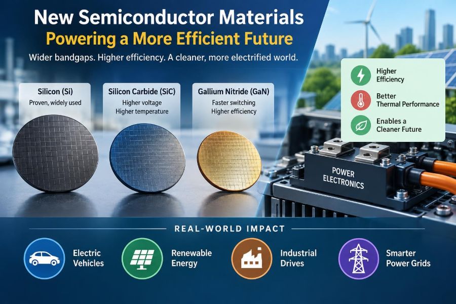
That is why new semiconductor materials have become central to power electronics. Devices built from silicon carbide, gallium nitride, and several emerging materials are changing what converters, drives, chargers, and grids can do.
The shift is not simply a contest to find a “better transistor.” It is a materials-and-system design problem involving losses, packaging, reliability, cost, control, and the real conditions in which equipment must operate.
⚡ Why Power Electronics Matter Everywhere
Power electronics converts and controls electrical energy. A power converter may change AC to DC, raise or lower voltage, create variable-frequency AC for a motor, or regulate battery charging.
These functions appear in laptop adapters, data centers, industrial motor drives, railway traction systems, renewable-energy inverters, electric vehicles, and utility infrastructure. Even a modest efficiency improvement can matter when a device operates continuously or handles large amounts of power.
Unlike a logic chip, which mainly processes information, a power semiconductor must repeatedly withstand substantial voltage and carry current. It must do so safely while generating manageable heat.
🧱 The Traditional Silicon Foundation
Silicon is still exceptionally capable. It is abundant, well understood, supported by mature manufacturing, and available in many device forms, including MOSFETs, IGBTs, diodes, and thyristors.
Its long development history also means engineers have extensive models, qualification methods, fabrication capacity, and packaging options. For many low- and medium-power designs, conventional silicon remains the most economical and sensible choice.
The material transition is therefore selective. New materials become attractive where their electrical and thermal properties solve a limitation that silicon-based devices cannot solve efficiently enough.
🔍 The Material Properties Behind Better Switches
A semiconductor’s usefulness in power conversion depends on several linked properties. Its bandgap is the energy required to move an electron from a bound state into a conducting state. A wider bandgap generally allows operation at higher temperature and stronger electric fields.
Engineers also examine critical electric field, carrier mobility, thermal conductivity, saturation velocity, and defect density. No single metric decides device quality; a material may be excellent in one property while creating challenges in another.
A useful analogy is building a bridge. Strength, weight, heat tolerance, manufacturability, and cost all matter. Choosing solely by one impressive specification can produce a poor overall structure.
🌡️ What “Wide-Bandgap” Really Means
Silicon carbide and gallium nitride are commonly called wide-bandgap semiconductors because their bandgaps are wider than silicon’s. This enables devices that can block higher voltages using thinner, more highly doped layers.
That structural advantage can lower the resistance of a high-voltage device when it is switched on. It can also support higher junction temperatures, although the complete module, package, capacitor, gate driver, and cooling system may impose lower practical limits.
Wide-bandgap does not mean indestructible. It means the material gives designers a different and often more favorable set of trade-offs.
📏 Blocking Voltage and Electric Field Strength
When a transistor is off, it must prevent current flow while supporting the applied voltage. This is called voltage blocking. The electric field inside the device must remain below the level that causes breakdown.
Silicon carbide can tolerate a much stronger electric field than silicon. In practical device structures, that means a SiC high-voltage drift region can be thinner than the equivalent silicon region.
A thinner drift region reduces resistance, especially at high voltage ratings. This is one reason SiC has become particularly relevant in equipment such as high-voltage traction inverters and fast DC chargers.
🔥 Conduction Loss Is Only Half the Story
When a switch is on, it dissipates power because voltage remains across it while current flows. In a MOSFET, this is often approximated by current squared multiplied by on-resistance. Higher current can therefore increase conduction loss very quickly.
But choosing the lowest advertised on-resistance is not always correct. A lower-resistance device may have larger capacitances, a larger package, a higher cost, or less favorable switching behavior.
Engineers must consider the entire operating range: load current, temperature, duty cycle, cooling conditions, and the time spent in each switching state.
⏱️ Why Fast Switching Changes Converter Design
A transistor loses energy during transitions because voltage and current overlap briefly while it turns on or off. Faster transitions can reduce that overlap and lower switching loss.
Gallium nitride devices are especially valued for rapid switching in many low- to medium-voltage applications. Their characteristics can enable power supplies to operate at higher switching frequencies than equivalent silicon designs.
Higher frequency can reduce the size of inductors, transformers, and filters. It does not automatically shrink every converter, however: electromagnetic interference, thermal design, and gate-drive constraints become more demanding as edge rates rise.
🪨 Silicon Carbide’s High-Voltage Strength
Silicon carbide, usually shortened to SiC, is a compound of silicon and carbon. Its combination of wide bandgap, high critical field, and good thermal conductivity makes it well suited to high-voltage, high-temperature power applications.
SiC MOSFETs and SiC Schottky diodes are now established options in several commercial converter categories. They can reduce losses in systems where silicon devices would otherwise need larger die areas, more cooling, or lower switching frequencies.
Typical application areas include electric-vehicle traction inverters, onboard chargers, DC fast chargers, photovoltaic inverters, industrial drives, and some grid-connected equipment.
🚗 Why SiC Fits Electric-Vehicle Systems
Electric vehicles place tight limits on mass, volume, battery energy, and cooling capacity. The traction inverter must efficiently create controlled AC for the motor, often from a high-voltage battery.
SiC can help reduce inverter switching and conduction losses under appropriate conditions. At the vehicle level, lower loss may reduce heat to be removed and can support smaller passive components or different cooling strategies.
Those system benefits are conditional, not automatic. Motor characteristics, switching frequency, battery voltage, drive cycle, control method, and component prices all influence whether SiC provides a worthwhile design advantage.
🔋 SiC in Chargers and Renewable Energy
Fast chargers and renewable-energy converters must process high power reliably for long periods. Their economics are affected by efficiency, enclosure size, installation requirements, and cooling hardware.
SiC’s voltage capability makes it attractive for high-voltage conversion stages. It can also allow engineers to raise switching frequency where doing so reduces magnetic-component size without creating excessive losses or noise.
For solar and energy-storage systems, the result can be a more compact power stage. Yet capacitors, contactors, protection circuits, isolation requirements, and grid rules still shape the final product.
💨 Gallium Nitride’s Speed Advantage
Gallium nitride, or GaN, has a wide bandgap and very high electron mobility in certain device structures. In power electronics, it is commonly used in high-electron-mobility transistors, often called HEMTs.
GaN power devices are particularly compelling where fast switching and compactness matter. Examples include USB-C adapters, server power supplies, telecom power converters, and some lower-voltage motor-control or energy-conversion stages.
Many commercial GaN devices are intended for voltage classes below the high-voltage territory where SiC is frequently used. The boundary is evolving as device structures and manufacturing improve.
🔌 How GaN Makes Smaller Chargers Possible
A charger must transfer energy through magnetic components, capacitors, switches, and control circuitry. When switching frequency rises, the transformer or inductor can often store and transfer the required energy with less physical material.
GaN devices can make high-frequency operation more practical because their switching losses can be low under well-designed conditions. This is a major reason compact, high-power-density adapters have become more feasible.
However, a smaller charger is not automatically a cooler charger. Reduced magnetic size may concentrate heat, and poor layout can create ringing, noise, or reliability problems. Compactness must be engineered rather than assumed.
🧭 SiC and GaN Serve Different Sweet Spots
It is tempting to frame SiC and GaN as direct rivals, but they often solve different problems. SiC is commonly selected where high blocking voltage, high current, and robust thermal behavior dominate. GaN is often selected where extremely fast switching and small size are priorities.
| Design consideration | Silicon carbide | Gallium nitride |
|---|---|---|
| Common strength | High-voltage, high-power conversion | High-frequency, compact conversion |
| Typical device focus | MOSFETs and Schottky diodes | HEMT-based power switches |
| Frequent applications | EV inverters, chargers, solar systems | Adapters, data-center supplies, telecom |
| Key design challenge | Cost, gate behavior, packaging and reliability | Fast-edge layout, gate control, thermal paths |
These are tendencies rather than rigid rules. The correct choice depends on voltage, power level, topology, switching frequency, cost target, and qualification requirements.
🧪 Device Structure Matters as Much as Chemistry
Material names alone do not predict final performance. A power device’s behavior depends on its layer structure, gate design, contacts, termination regions, passivation, die layout, and package.
For example, two transistors made from the same semiconductor can differ substantially in threshold behavior, capacitance, short-circuit robustness, reverse-conduction behavior, and susceptibility to switching stress.
Engineers should read data sheets as descriptions of specific devices under defined test conditions, not as universal statements about an entire material family.
🧊 Thermal Conductivity and the Heat Path
Heat starts in the semiconductor junction but must travel through the die attach, substrate, package, thermal interface material, heat sink, and eventually the surrounding air or liquid. A material with favorable thermal conductivity helps, but it cannot compensate for a poor thermal path.
Junction temperature strongly affects electrical resistance, lifetime, and operating margin. Repeated temperature cycling can also fatigue solder joints, bond wires, and interfaces.
A credible thermal design therefore uses measured or modeled losses, realistic cooling conditions, and transient as well as steady-state operation. A device that survives a brief laboratory test may still struggle in continuous field service.
📦 Packaging Has Become a Performance Limiter
As switching devices become faster, package inductance becomes more significant. Stray inductance creates voltage overshoot when current changes rapidly, according to the relationship between inductance and rate of current change.
Modern power modules address this with compact current loops, low-inductance interconnects, improved substrates, and in some cases advanced bonding methods. Packaging is no longer merely a protective shell around the die.
For wide-bandgap devices, package choice can determine whether the theoretical material advantage reaches the converter terminals.
🌀 Fast Edges Create EMI Challenges
Fast voltage transitions are useful for reducing switching loss, but they also excite parasitic capacitances and inductances. The resulting ringing can increase voltage stress and produce electromagnetic interference, or EMI.
EMI can disrupt nearby signals, complicate compliance testing, and increase filter requirements. In isolated converters, common-mode currents through transformer capacitance can become a significant concern.
- Minimize high-current switching-loop area.
- Place decoupling capacitors close to the switching devices.
- Use controlled gate resistance or active gate control where appropriate.
- Measure with probes and grounding methods suitable for fast transients.
Slowing a switch slightly may sometimes improve the overall design by reducing overshoot and filter burden, even if it adds a small amount of switching loss.
🎛️ Gate Driving Is Not a Detail
The gate driver determines how a power transistor moves between off and on states. Its supply voltage, source and sink current, loop inductance, isolation, timing, and protection features all influence converter behavior.
Wide-bandgap devices can be less forgiving of careless gate-drive design because their switching transitions are fast. Gate-loop inductance can cause oscillation, false turn-on, or excessive voltage stress.
Designers should follow the device manufacturer’s recommended gate-voltage limits closely, then validate operation on the actual printed-circuit board. A simulation cannot capture every parasitic element in a real layout.
🛡️ Reliability Requires More Than a Good Efficiency Plot
Efficiency measurements often describe a narrow set of operating points. Reliability asks a broader question: how will the device and package behave after years of temperature cycling, voltage stress, humidity exposure, vibration, overloads, and switching events?
Important mechanisms can include gate-oxide wear, threshold-voltage shift, bond fatigue, dielectric stress, and degradation caused by defects. The details vary between SiC, GaN, silicon, device architecture, and manufacturer.
Qualification data and field history matter, particularly in automotive, aerospace, medical, industrial, and grid applications. A lower-loss switch is valuable only if its expected lifetime fits the equipment’s service requirement.
⚠️ Short Circuits and Fault Behavior
Power converters must survive or safely interrupt abnormal events such as short circuits, shoot-through in a bridge leg, load faults, and overvoltage transients. The fault response of a switch is as important as its normal operating behavior.
Some SiC devices can have shorter short-circuit withstand times than engineers may expect from familiar silicon IGBTs. Fast detection and coordinated protection are therefore essential in relevant topologies.
Protection design may include desaturation sensing, current sensing, soft shutdown, gate clamping, fuses, contactors, and controller-based fault logic. The correct combination depends on the system’s energy source and fault-clearing capability.
💰 Cost Must Be Evaluated at System Level
A wide-bandgap transistor may cost more than a silicon alternative, especially when compared only by device price. But the full system may need fewer parallel devices, smaller magnetics, less cooling, or a smaller enclosure.
Conversely, a premium switch can create new expenses in drivers, PCB materials, EMI filtering, testing, and qualification. The system-level answer is not always favorable.
A useful comparison includes component cost, assembly, heat sink, magnetics, filter size, enclosure, expected energy loss, manufacturing yield, and service implications. This avoids optimizing one line item while increasing the real product cost.
🏭 Manufacturing Defects Still Shape Progress
Semiconductor materials are grown as crystals or deposited as layers before devices are fabricated. Crystal defects, impurities, wafer uniformity, and interface quality can affect yield, breakdown behavior, leakage, and long-term stability.
SiC manufacturing has advanced substantially, but producing high-quality wafers remains more challenging than producing conventional silicon wafers. GaN also has manufacturing choices involving substrates and epitaxial growth that influence performance and cost.
Many material “discoveries” become commercially meaningful only after manufacturing processes make them repeatable at sufficient scale.
🔬 Diamond and Gallium Oxide: Promising, Not Mainstream
Diamond has extraordinary thermal conductivity and a very wide bandgap, which makes it scientifically attractive for extreme power and temperature conditions. Its practical use is constrained by difficult and expensive material processing, doping, contacts, and device fabrication.
Gallium oxide offers a very wide bandgap and potentially economical native substrates. Its relatively low thermal conductivity creates a serious thermal-management challenge, especially in high-power devices.
These materials are active research and development areas, but they should not be treated as direct replacements for silicon, SiC, or GaN in ordinary designs. Laboratory potential and mature product readiness are different stages.
🧬 Aluminum Nitride and Ultra-Wide-Bandgap Research
Researchers also investigate aluminum nitride, aluminum gallium nitride alloys, boron nitride, and other ultra-wide-bandgap materials. Their appeal lies in their theoretical ability to withstand very high fields and temperatures.
The obstacles are formidable: controlled doping, low-resistance contacts, crystal quality, defect management, thermal integration, and repeatable fabrication. A material can possess excellent intrinsic properties yet remain unsuitable for commercial devices.
For students, the key lesson is that semiconductor innovation is a chain. Progress in the crystal, interface, process, package, circuit, and test method must align.
🌐 Power Electronics Is Moving Toward Higher Voltage
Higher DC bus voltages can reduce current for a given power level. Since resistive loss in cables and conductors scales with current squared, this can reduce distribution losses or permit lighter conductors.
This trend helps explain interest in higher-voltage vehicle architectures, charging infrastructure, renewable-energy systems, and data-center power distribution. It also increases insulation, clearance, protection, and safety demands.
Wide-bandgap devices do not create the high-voltage trend by themselves, but they can make certain high-voltage conversion stages more efficient and compact.
🖥️ Data Centers Need Efficient Conversion Too
Data centers contain many layers of conversion: utility AC, backup power, distribution buses, server power supplies, and point-of-load regulators. Loss at each stage becomes heat that must often be removed by additional energy-consuming cooling equipment.
GaN can be attractive in high-frequency server power supplies, while SiC may fit higher-power front-end or infrastructure-level stages. The exact split depends on voltage level and architecture.
Here, power density matters alongside efficiency. A smaller, cooler power supply can free space for computing equipment, but reliability and serviceability remain non-negotiable.
🧰 Choosing a Material for a New Design
Start with the application rather than a preferred material. Define the required input and output voltage, power range, switching frequency, allowable temperature, lifetime, space limits, acoustic limits, and cost ceiling.
- Select a converter topology suitable for the electrical task.
- Estimate conduction, switching, magnetic, capacitor, and auxiliary losses.
- Assess thermal paths and fault conditions.
- Compare silicon, SiC, and GaN devices at realistic operating points.
- Prototype the layout and verify waveforms, EMI, temperature, and protection behavior.
This sequence prevents the common mistake of selecting an advanced transistor first and trying to force the rest of the design around it.
📐 Measurement Mistakes With Fast Power Devices
Fast-switching circuits are easy to measure badly. A long oscilloscope probe ground lead can add inductance and display ringing that is partly created by the measurement setup itself.
Voltage probes, current probes, bandwidth settings, probe placement, and isolation methods all affect results. Measurements should be interpreted with the circuit’s expected parasitics in mind.
Another common error is testing at one convenient load point and extrapolating too broadly. Losses, ringing, and thermal behavior can change significantly across input voltage, load current, temperature, and operating mode.
🧠 Control Algorithms Must Keep Up
Higher switching frequency can give control designers more opportunities to adjust duty cycle or current, but it also shortens available computation and sensing time. Noise from fast transitions can contaminate measurements if sampling is poorly timed.
Digital controllers need carefully designed dead time, current sensing, protection thresholds, and compensation. Dead time that is too long increases loss and distortion; too little can cause destructive cross-conduction.
Material advances and control advances reinforce each other. A capable switch needs equally capable sensing, firmware, and fault handling.
🌱 Efficiency Is a Resource Question
Reducing conversion loss can lower electricity use and thermal load, particularly in equipment that runs frequently or at high power. It can also reduce the amount of cooling hardware required.
Yet sustainability should be assessed broadly. Material extraction, wafer processing, manufacturing yield, product lifetime, repairability, and end-of-life handling all affect environmental impact.
The most responsible choice is usually the device that meets the required performance and durability with the least total system burden, not necessarily the newest material.
🎓 Skills Engineers Need in This Transition
Working with emerging power semiconductors requires more than semiconductor physics. Engineers benefit from competence in converter topologies, PCB layout, magnetics, thermal modeling, EMC, embedded control, measurement practice, and safety.
Students can build these skills by comparing device data sheets, simulating a converter, constructing low-voltage prototypes, and learning to correlate predicted waveforms with measured results. Working professionals can apply the same mindset through disciplined design reviews and test plans.
The durable skill is systems thinking: recognizing that material properties influence the circuit, and the circuit influences the package, layout, controls, cost, and reliability.
🔮 What to Watch Next
The next advances may not always arrive as a dramatic new material. They may emerge as lower-defect wafers, more robust gate structures, improved module interconnects, integrated drivers, better thermal substrates, or designs that reduce parasitic inductance.
Researchers and manufacturers are also improving normally-off behavior, high-voltage capability, ruggedness, and production consistency. These practical refinements often determine whether an exciting device becomes widely useful.
For designers, it is wise to watch validated device data, package innovations, and application-specific reference designs rather than relying only on headline material properties.
✅ The Core Takeaway: Match Material to the System
Silicon continues to serve power electronics extremely well. SiC is reshaping many high-voltage and high-power applications, while GaN is enabling compact, fast-switching converters in important lower- and medium-voltage domains.
The major discovery is not that one material wins every application. It is that wider-bandgap materials expand the design space: they can support higher voltage, faster switching, higher temperature capability, or smaller passive components when the surrounding system is designed to use those strengths.
Successful power electronics will come from matching semiconductor material, device structure, package, topology, layout, controls, protection, and economics to the actual job.
Semiconductor materials are changing power electronics because they let engineers trade energy loss, size, voltage capability, and thermal performance in new ways—but only disciplined system design turns that potential into dependable equipment. 🔌⚡🌍